


Page 88 - Read Online
P. 88
Zhou et al. Soft Sci. 2026, 6, 10                                                 Page 25 of 47


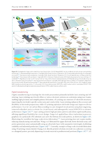
               Figure 13. Strategies for large-scale manufacturing of electrodes. (A) GO-based MEG can be produced at scale using screen printing
               technology [173] . Reproduced with permission. Copyright 2018, Royal Society of Chemistry; (B) Screen printing technology for integrated
               electrodes [34] . Reproduced with permission. Copyright 2025, Royal Society of Chemistry; (C) Circuit made by laser etching carbon film
               technology [33] . Reproduced with permission. Copyright 2025, American Chemical Society; (D) Electrodes prepared by laser printing on PI
               substrate [109] . Reproduced under CC BY license from Su Yang, 2024, Nature Communications; (E) Manufacturing of electrode arrays by
               nano-ultraviolet laser processing [105] . Reproduced with permission. Copyright 2021, Springer Nature Limited; (F) Schematic diagram of
               mass production by 3D printing technology [153] . Reproduced with permission. Copyright 2023, John Wiley & Sons. GO: Graphene oxide;
               MEG: moisture-electric generator; PI: polyimide; 3D: three-dimensional; MWCNTs: multi-walled carbon nanotubes; PEDOT:PSS:
               poly(3,4-ethylenedioxythiophene):poly(styrenesulfonate); H-PSS: poly(4-styrene sulfonic acid).


               Digital manufacturing
               Digital manufacturing technology for electrode preparation primarily includes laser printing and 3D
               printing. Laser printing can directly ablate or induce electrode patterns on a substrate using laser beams,
               enabling high-precision and complex pattern fabrication. 3D printing can construct 3D electrode structures,
               improving the electrode’s specific surface area and conductivity. Laser printing enhances the accuracy and
               flexibility of electrode preparation, while 3D printing optimizes electrode design and improves device
               performance. Yu et al. cut carbon film according to a pre-designed circuit pattern using laser engraving,
               removed redundant parts to obtain the circuit layout, and subsequently coated MWCNTs to enhance
               performance [Figure 13C] . Laser cutting achieves high-precision patterns and allows rapid modification,
                                     [33]
               offering significant flexibility for circuit design. Yang et al. applied laser direct induction to generate
               graphene on a polyimide (PI) substrate and carve the bottom electrode pattern, as shown in Figure 13D,
               illustrating the workflow for large-scale device fabrication [109] . Laser printing does not require molds,
               reducing manufacturing cost and time. Wang et al. fabricated the upper electrode, lower electrode array, and
               power generation array automatically using an ultraviolet laser with nanometer wavelength, facilitating
               scalability and industrial production [Figure 13E] . Currently, examples of large-scale electrode fabrication
                                                        [105]
               using 3D printing remain limited. Huang et al. directly printed a bottom electrode on a substrate according
               to a designed pattern, precisely depositing electrode material at predetermined positions [Figure 13F] . 3D
                                                                                                    [153]

