
Page 80 - Read Online
P. 80
Page 4 of 10 Li et al. Microstructures 2023;3:2023007 https://dx.doi.org/10.20517/microstructures.2022.27
RESULTS AND DISCUSSION
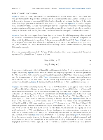
Figure 2A shows the GIXRD patterns of PZO-based films at 2θ = 20°-60°. In the case of a PZO-based film
with good crystallinity, the perovskite crystalline structure is orthorhombic phase, and no secondary phase
is detectable in the range of accuracy of GIXRD technology. In order to investigate the effect of Bi doping in
PZO, the enlarged patterns of PZO-based films at 2θ = 30°-31° are shown in Figure 2B. The diffraction peak
(122) around 30.5° of PBZ and PZB compared to pure PZO has a slight shift towards the low angle and high
angle, respectively, which demonstrates Bi successfully replaces Pb and Zr at A/B-sites. In terms of the
[15]
change in diffraction peak, similar phenomena have been observed in La-doped PZO films at low content .
Figure 3A shows the SEM images of PZO-based films. It can be seen that all films possess good density and
no pores and crack in the surface morphology. The grain size of PZB films exceeds PBZ and pure PZO
films, which should be related to a reduced Pb/Zr ratio compared to PZO and PBZ. Figure 3B displays the
AFM images of PZO-based films. The surface roughness R is 2.91 nm, 3.32 nm, and 4.04 nm for pure PZO,
q
PBZ, and PZB films. PZO-based thin films are characterized by a smooth and flattened surface, indicating
high-quality materials.
3+
4+
Due to the valence difference of Bi , Pb and Zr , the chemical defect would be generated. The defect
2+
equation of Bi replaces Pb and Zr is given as follows:
It can be seen that the point defect of and could be generated when Bi acts as a donor and acceptor
dopant, respectively. Figure 4 shows the room temperature frequency dependency of dielectric properties
for PZO-based films. As frequency increases, the dielectric properties of PZO-based films maintain stability
over the frequency range of 1 kHz-1 MHz. Figure 4A shows that the dielectric constant enhances from ~250
for PZO films to ~325 for PBZ and PZB films, which may be related to an increased point defect
contribution. In addition, Figure 4B illustrates that the dielectric losses of PZO-based films are around 0.1.
Figure 5A shows the room temperature P-E loops of PZO-based films at an applied electric field of
800 kV/cm. PZO films exhibit an apparent double hysteresis loop. Bi-doped PZO films at A/B sites still
show double hysteresis loops, but the polarization and switching fields have been changed. The polarization
differences Δ P between P and P of PZO-based films are exhibited in Figure 5C. The P of all PZO-based
max
r
r
films is unchanged, but the P of Bi-doped PZO films is lower than that of pure PZO films. Therefore, Δ P
max
of Bi-doped PZO films cannot be enhanced effectively at the same electric field. Figure 5B shows the I-E
loops of PZO-based films at an applied electric field of 800 kV/cm. Four current peaks correspond to the
AFE-to-FE and FE-to-AFE phase transition, respectively [8,10] . Compared to pure PZO films, PBZ and PZB
films both possess a lower current density and higher forward switching field E of 562.2 kV/cm for PBZ
F
and 537.3 kV/cm for PZB than 413.5 kV/cm for PZO films, which illustrates Bi-doping enhances
antiferroelectricity of PZO materials in some degree. As discussed above, this result may be related to a
reduction in t value to stabilize the AFE phase. Unfortunately, the increased Δ E value sacrifices the E of
F
PBZ and PZB, as shown in Figure 5D. It can be attributed to an enlarged grain size [Figure 3], which differs
from the previous results. As grain size decreases, hysteresis loss in relaxor ferroelectric materials and
antiferroelectric materials is reduced due to increased dipole mobility, and therefore PBZ and PZB with
large grain sizes would possess a high Δ E. It can be seen that the antiferroelectricity of PZO is no positive