
Page 81 - Read Online
P. 81
Li et al. Microstructures 2023;3:2023007 https://dx.doi.org/10.20517/microstructures.2022.27 Page 5 of 10
Figure 2. (A) The GIXRD patterns of PZO-based films at 2θ range from 20° to 60°. (B) The enlarged patterns at 2θ =30°-31°.
GIXRD: Grazing incident X-ray diffraction; PZO: PbZrO .
3
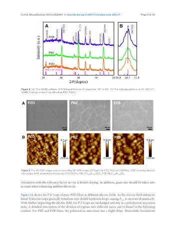
Figure 3. The (A) SEM images and corresponding (B) AFM images (5*5 μm) for PZO, PBZ, and PZB films. SEM: Scanning electron
microscope; AFM: atomic force microscopy; PZO: PbZrO ; PBZ: (Pb Bi )ZrO ; PZB: Pb(Zr Bi )O .
3 0.95 0.05 3 0.95 0.05 3
correlation with the tolerance factor in t in A/B-sites doping. In addition, grain size should be taken into
account when enhancing antiferroelectricity.
Figure 6A shows the P-E loops of pure PZO films at different electric fields. As the electric field enhances,
linear hysteresis loops gradually transform into double hysteresis loops causing P to increase dramatically.
max
With further improving the electric field, the P-E loops are unchanged and stay in a polarization saturation
state. A detailed description of the division of regions into different states can be found in the following
content. For PBZ and PZB films, the polarization saturation has a slight delay. Meanwhile, breakdown