
Page 157 - Read Online
P. 157
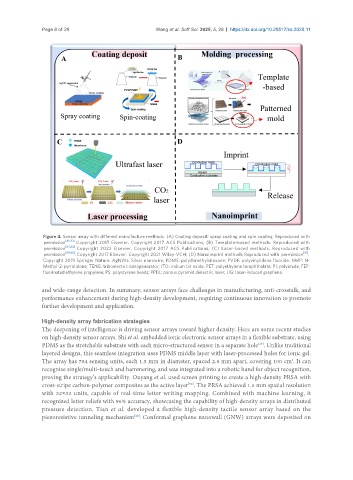
Page 8 of 29                           Wang et al. Soft Sci. 2025, 5, 28  https://dx.doi.org/10.20517/ss.2025.11


                Figure 4. Sensor array with different manufacture methods. (A) Coating deposit: spray coating and spin coating. Reproduced with
                permission [80,81] . Copyright 2017 Elsevier. Copyright 2017 ACS Publications; (B) Template-based methods. Reproduced with
                permission [83,84] . Copyright  2023  Elsevier.  Copyright  2017  ACS  Publications;  (C)  Laser-based  methods.  Reproduced  with
                permission [89,90] . Copyright 2017 Elsevier. Copyright 2021 Wiley-VCH; (D) Nanoimprint methods Reproduced with  permission [91] .
                Copyright 2019 Springer Nature. AgNWs: Silver nanowire; PDMS: polydimethylsiloxane; PVDF: polyvinylidene fluoride; NMP: N-
                Methyl-2-pyrrolidone; TENG: triboelectric nanogenerator; ITO: indium tin oxide; PET: polyethylene terephthalate; PI: polyimide; FEP:
                fluorinated ethylene propylene; PS: polystyrene beads; PPDL: porous pyramid dielectric layer; LIG: laser-induced graphene.

               and wide-range detection. In summary, sensor arrays face challenges in manufacturing, anti-crosstalk, and
               performance enhancement during high-density development, requiring continuous innovation to promote
               further development and application.

               High-density array fabrication strategies
               The deepening of intelligence is driving sensor arrays toward higher density. Here are some recent studies
               on high-density sensor arrays. Shi et al. embedded ionic electronic sensor arrays in a flexible substrate, using
                                                                                        [27]
               PDMS as the stretchable substrate with each micro-structured sensor in a separate hole . Unlike traditional
               layered designs, this seamless integration uses PDMS middle layer with laser-processed holes for ionic gel.
               The array has 784 sensing units, each 1.5 mm in diameter, spaced 2.8 mm apart, covering 100 cm . It can
                                                                                                   2
               recognize single/multi-touch and hammering, and was integrated into a robotic hand for object recognition,
               proving the strategy’s applicability. Ouyang et al. used screen printing to create a high-density PRSA with
               cross-stripe carbon-polymer composites as the active layer . The PRSA achieved 1.5 mm spatial resolution
                                                                [92]
               with 32×32 units, capable of real-time letter writing mapping. Combined with machine learning, it
               recognized letter reliefs with 96% accuracy, showcasing the capability of high-density arrays in distributed
               pressure detection. Tian et al. developed a flexible high-density tactile sensor array based on the
               piezoresistive tunneling mechanism . Conformal graphene nanowall (GNW) arrays were deposited on
                                              [28]