
Page 156 - Read Online
P. 156
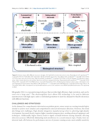
Wang et al. Soft Sci. 2025, 5, 28  https://dx.doi.org/10.20517/ss.2025.11        Page 7 of 29


                Figure 3. Sensor arrays with different structure designs. (A) Symmetrical electrode sensor array. Reproduced with  permission [72] .
                                                                                        [73]
                Copyright 2016 ACS Publication; (B) Independent electrode flexible electronics. Reproduced with permission  . Copyright 2022 AAAS;
                                                             [74]
                (C) Cross-layer electrode sensor array. Reproduced with permission  . Copyright 2021 Wiley-VCH; (D) Regular microstructure sensor
                                                                                           [75-77]
                array: micro-dome structure; micropillars structure and micro-pyramid structure, Reproduced with  permission  . Copyright 2020
                Wiley-VCH. Copyright 2014 ACS Publications. Copyright 2024 Wiley-VCH; (E) Bioinspired structure sensor array: cilia-based e-skin
                                                        [78,79]
                and fingerprint microstructures, Reproduced with permission  . Copyright 2025 OAE Publishing. Copyright 2018 Springer Nature. PI:
                Polyimide; MAB e-skin: micropyramid array bimodal electronic skin; e-skin: electronic skin; PDMS: polydimethylsiloxane; PVA: polyvinyl
                alcohol.
               lithography (NIL) is a nanopatterning technique that provides high efficiency, high resolution, and can be
               used over a large area . The electrocapillary force allows NIL technology to be used to fabricate
                                    [91]
               nanostructures with high aspect ratios or deformed geometries to meet the demand for flexible electronics
               with different functions.


               CHALLENGES AND STRATEGIES
               As the demand for comprehensive information acquisition grows, sensor arrays are moving towards higher
               density to achieve more detailed and comprehensive external information detection. However, this trend
               also brings new challenges. High-density integration manufacturing is key to achieving high-density
               development. Increased density requires higher manufacturing precision, needing advanced equipment and
               techniques. Additionally, higher density leads to signal crosstalk between sensing channels, affecting
               detection accuracy. Effectively eliminating such interference is a crucial research topic. Finally, there are
               inherent trade-offs between the performance metrics of pressure sensing arrays, most notably sensitivity