


Page 65 - Read Online
P. 65
Page 10 of 16                                               Dong et al. Energy Mater.  2026, 6, 600026


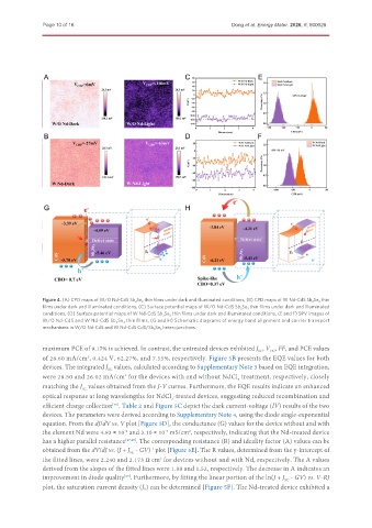
               Figure 4. (A) CPD maps of W/O Nd-CdS Sb 2 Se 3  thin films under dark and illuminated conditions, (B) CPD maps of W Nd-CdS Sb 2 Se 3  thin
               films under dark and illuminated conditions, (C) Surface potential maps of W/O Nd-CdS Sb 2 Se 3  thin films under dark and illuminated
               conditions, (D) Surface potential maps of W Nd-CdS Sb 2 Se 3  thin films under dark and illuminated conditions, (E and F) SPV images of
               W/O Nd-CdS and W Nd-CdS Sb 2 Se 3  thin films, (G and H) Schematic diagrams of energy band alignment and carrier transport
               mechanisms in W/O Nd-CdS and W Nd-CdS CdS/Sb 2 Se 3  heterojunctions.

               maximum PCE of 9.17% is achieved. In contrast, the untreated devices exhibited J , V , FF, and PCE values
                                                                                    SC
                                                                                       OC
               of 28.60 mA/cm , 0.424 V, 62.27%, and 7.55%, respectively. Figure 5B presents the EQE values for both
                             2
               devices. The integrated J  values, calculated according to Supplementary Note 3 based on EQE integration,
                                    SC
               were 28.50 and 26.02 mA/cm  for the devices with and without NdCl  treatment, respectively, closely
                                         2
                                                                             3
               matching the J  values obtained from the J-V curves. Furthermore, the EQE results indicate an enhanced
                           SC
               optical response at long wavelengths for NdCl -treated devices, suggesting reduced recombination and
                                                        3
               efficient charge collection . Table 2 and Figure 5C depict the dark current-voltage (IV) results of the two
                                     [46]
               devices. The parameters were derived according to Supplementary Note 4, using the diode single-exponential
               equation. From the dJ/dV vs. V plot [Figure 5D], the conductance (G) values for the device without and with
               the element Nd were 4.93 × 10  and 3.10 × 10  mS/cm , respectively, indicating that the Nd-treated device
                                         -2
                                                              2
                                                      -3
               has a higher parallel resistance [47,48] . The corresponding resistance (R) and ideality factor (A) values can be
               obtained from the dV/dJ vs. (J + J  - GV)  plot [Figure 5E]. The R values, determined from the y-intercept of
                                                 -1
                                           SC
               the fitted lines, were 2.240 and 2.173 Ω cm  for devices without and with Nd, respectively. The A values
                                                    2
               derived from the slopes of the fitted lines were 1.88 and 1.52, respectively. The decrease in A indicates an
               improvement in diode quality . Furthermore, by fitting the linear portion of the ln(J + J  - GV) vs. V-RJ
                                         [49]
                                                                                            SC
               plot, the saturation current density (J 0) can be determined [Figure 5F]. The Nd-treated device exhibited a

