


Page 62 - Read Online
P. 62
Dong et al. Energy Mater.  2026, 6, 600026                                        Page 7 of 16


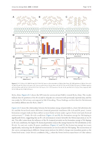
               Figure 2. (A-C) Effect of W Nd-CdS and W/O Nd-CdS layers on the orientation of Sb 2 Se 3  thin films, (D) XRD patterns of Sb 2 Se 3  films with
               W Nd-CdS and W/O Nd-CdS layers, (E) Texture coefficients of Sb 2 Se 3  films with W Nd-CdS and W/O Nd-CdS layers, (F) Raman spectra
               of Sb 2 Se 3  films with W Nd-CdS and W/O Nd-CdS layers, (G-I) XPS spectra of Sb 3d, Se 3d, and Nd 3d for Sb 2 Se 3  films prepared with
               W Nd-CdS and W/O Nd-CdS layers.


               Sb Se  films. Figure 2G-I shows the XPS data for untreated and NdCl -treated Sb Se  films. The results
                 2
                   3
                                                                                       2
                                                                                          3
                                                                             3
               indicate that the positions of the Sb 3d and Se 3d peaks are consistent with previously reported data, and the
               two peaks for Nd 3d may correspond to Nd-O bonding. These findings confirm that the Nd element
               successfully diffuses into the Sb Se  films .
                                                 [38]
                                         2
                                           3
               Figure 3A-D shows the relationship between the formation energy of point defects, where Nd substitutes for
               Sb, and the Fermi level under different chemical potential conditions (Sb-rich and Sb-poor). Lower
               formation energies indicate that a defect is more likely to form under a given Fermi level and chemical
               environment . Under Sb-rich conditions [Figure 3A and B], the formation energy for Nd doping is
                           [39]
               significantly lower, suggesting that an Sb-rich environment is more favorable for Nd incorporation at the Sb
               site. This effect arises from the influence of the Sb chemical potential on the formation energy of Nd doping:
               in Sb-rich conditions, the higher Sb chemical potential reduces the energy barrier for Nd substitution at the
               Sb site. In contrast, under Sb-poor conditions [Figure 3C and D], the formation energy increases
               significantly, indicating that Sb-depleted environments are less favorable for Nd doping. The intersections of
               the curves corresponding to different charge states indicate the defect’s charge state transition points as the
               Fermi level varies. Under Sb-rich conditions (Nd ), when the Fermi level increases from 0 eV (the valence
                                                         Sb1

