


Page 61 - Read Online
P. 61
Page 6 of 16                                                Dong et al. Energy Mater.  2026, 6, 600026


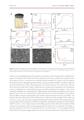
               Figure 1. (A) Schematic diagram illustrating the deposition of Nd-incorporated CdS thin films, (B) XRD patterns of W Nd-CdS and W/O
               Nd-CdS samples, (C) Transmittance spectra, (D-F) XPS spectra of Cd 3d, S 2p, and Nd 3d, (G and H) Surface SEM images of W Nd-CdS
               and W/O Nd-CdS samples, (I) TAS spectra of W Nd-CdS and W/O Nd-CdS samples.


               influences the crystallographic growth and preferred orientation of the subsequent Sb Se  absorber layer.
                                                                                            3
                                                                                          2
               Figure 2A-C illustrates the evolution of the Sb Se  absorber layer for the two sample sets: (a) under the W/O
                                                        3
                                                      2
               Nd condition, the Sb Se  nucleates with an essentially random orientation; (b-c) under the W Nd condition,
                                2
                                   3
               Nd diffuses into Sb Se  during film growth, inducing a pronounced preferential [hk1] orientation. Figure 2D
                                 3
                               2
               shows the XRD patterns of Sb Se  thin films grown under both conditions. The results indicate that the
                                            3
                                         2
               Sb Se  films grown under both conditions exhibit the same crystal structure, belonging to the orthorhombic
                 2
                   3
               system. A magnified view of the XRD patterns is provided in Supplementary Figure 7. The texture
               coefficients of the films were calculated from the XRD patterns, and the results are presented as a bar chart in
               Figure 2E. Since Sb Se  has a typical (Sb Se )  ribbon-like structure, the carrier transport is most efficient
                                                    6 n
                                                 4
                                  3
                               2
               when the ribbon structure is perpendicular to the substrate, and least efficient when they are parallel . The
                                                                                                    [35]
               data show that Sb Se  films grown under the Nd treatment condition (W Nd) have higher texture coefficients
                                3
                             2
               on the (211), (221), and (301) planes compared to films grown without Nd (W/O Nd). This phenomenon
               indicates that the [hk1] orientation is favored during growth, which facilitates improved carrier transport
               (JCPDS card No. 15-0861). Figure 2F presents the Raman spectra of Sb Se  films with and without NdCl 3
                                                                               3
                                                                             2
               treatment. Two prominent peaks, located at approximately 188 and 208 cm , are observed. These peaks are
                                                                               -1
               typically attributed to the Sb-Se-Sb bending vibrations in the Sb Se  films [36,37] . The strengthened Raman
                                                                       2
                                                                          3
               features after Nd treatment suggest improved structural order and reduced defect-related disorder in the

