


Page 63 - Read Online
P. 63
Page 8 of 16                                                Dong et al. Energy Mater.  2026, 6, 600026


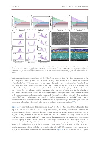
               Figure 3. (A-D) Relationship between point defects and the Fermi level in Nd-doped Sb 2 Se 3  thin films under different chemical potential
               conditions (Sb-rich and Sb-poor), (E) Variation in Se/Sb/Nd contents in Sb 2 Se 3  samples at different etching depths, (F and G) Surface
               morphology of Sb 2 Se 3  films with W Nd-CdS and W/O Nd-CdS, (H and I) Cross-sectional images of Sb 2 Se 3  films with W Nd-CdS and W/O
               Nd-CdS.


               band maximum) to approximately 0.5 eV, the Nd defect transitions from Nd  (high charge state) to Nd +
                                                                                  3+
               (low charge state). Similarly, under Sb-rich conditions (Nd ), the transition from Nd  to Nd  occurs around
                                                                                             +
                                                                                       3+
                                                                Sb2
               a Fermi level of 0.6 eV. These transition points suggest that under p-type conditions (low Fermi level), the
               high charge state (Nd ) is more stable, while under n-type conditions (high Fermi level), the low charge state
                                 3+
                               0
               (such as Nd  or Nd ) is more stable. Overall, the analysis indicates that Nd  doping has the lowest formation
                         +
                                                                             3+
               energy under Sb-rich conditions, making it more favorable for doping behavior. Additionally, a low Fermi
               level (p-type conditions) stabilizes the Nd  state, suggesting that Nd doping can be promoted by introducing
                                                  3+
               an Sb-rich environment and controlling the Fermi level. It should be noted that, although hybrid functionals
               such as HSE06 may still underestimate absolute bandgap values compared with GW calculations or
               experimental results, the relative trends in defect formation energies and charge-state stability discussed here
               are expected to be robust with respect to the choice of exchange-correlation functional [40,41] .
               Figure 3E presents the high-resolution depth-profile XPS spectra of NdCl -treated Sb Se  films at etching
                                                                               3
                                                                                         2
                                                                                            3
               depths of 0, 50, 100, and 150 nm. In the Se 3d region, the Se 3d  and Se 3d  peaks remain clearly defined
                                                                               3/2
                                                                     5/2
               across all depths, indicating a stable Se chemical state throughout the film. In the Sb 3d region, the main Sb
               3d  and Sb 3d  peaks dominate, while a minor Sb-O shoulder is observed solely at the 0 nm depth,
                            3/2
                 5/2
               signifying surface-confined oxidation . As the etching depth increases beyond 0 nm, the Sb-O component
                                               [42]
               decreases rapidly, indicating that the bulk film is essentially unoxidized. In the Nd 3d region, clear Nd 3d
               peaks appear at each depth, and the Nd atomic concentration increases progressively with depth, thereby
               verifying that Nd diffuses inward from the heterojunction interface into the Sb Se  film rather than
                                                                                           3
                                                                                        2
               remaining as a superficial layer. To further investigate the effect of NdCl  treatment on the morphology of
                                                                             3
               Sb Se  films, surface SEM characterization was first performed. Figure 3F and G shows that the Sb Se  grains
                                                                                                  2
                                                                                                    3
                   3
                 2

