


Page 66 - Read Online
P. 66
Dong et al. Energy Mater.  2026, 6, 600026                                       Page 11 of 16


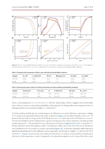
               Figure 5. (A) J-V curves, (B) EQE spectra, (C) dark J-V curves, (D) dJ/dV vs. V graph for G extraction, (E) dV/dJ vs. (J + J SC  - GV)  graph for
                                                                                                   -1
               R and A extraction, and (F) ln(J + J SC  - GV) vs. V-RJ graph for J0 extraction, for samples without and with NdCl 3  treatment.

               Table 1. The photovoltaic parameters of Sb 2 Se 3  solar cells without and with NdCl 3  treatment

               Sample      V OC  (V)  J SC  (mA/cm )  FF (%)     Efficiency (%)  R S  (ohm)   R SH  (ohm)
                                              2
               W/O Nd      0.424      28.60           62.27      7.55            114.83       13,014
               W Nd        0.465      30.54           64.58      9.17            110.48       19,782


               Table 2. Electrical parameters related to the diode and interface for devices without and with NdCl 3  treatment

               Sample      G (mS/cm )      R (Ω cm )    A      J0 (mA/cm )      W d  (nm)   N trap  (cm )
                                  2
                                                                      2
                                                                                                  -3
                                                 2
               W/O Nd      4.93 × 10 -2    2.24         1.88   1.81 × 10 -3     216.44      2.98 × 10 14
               W Nd        3.10 × 10 -3    2.173        1.52   9.42 × 10 -5     307.60      1.76 × 10 14
               lower J 0, decreasing from 1.81 × 10  to 9.42 × 10  mA/cm . In principle, a lower J 0 suggests fewer shunt paths
                                                               2
                                                       -5
                                            -3
               and a reduced carrier recombination probability, indicating that Nd doping effectively mitigates the loss of
               photogenerated carriers and favors higher V  formation .
                                                              [50]
                                                    OC
               To better understand the factors contributing to the differences in carrier lifetimes, capacitance-voltage
               (C-V) analysis was also performed in this study. As shown in Figure 6A, the Mott-Schottky curves (1/C -V)
                                                                                                       2
               indicate that the built-in voltage of the W/O Nd device is 0.474 V, while that of the W Nd device is 0.530 V.
               The increased built-in electric field provides a greater driving force for carrier separation, resulting in faster
               charge separation . The parameters were calculated according to Supplementary Note 5 using the C-V
                              [51]
               fitting method to extract the depletion width. The depletion widths (W ) of the W/O Nd and W Nd devices
                                                                           d
               were calculated to be 216.44 and 307.60 nm, respectively [Figure 6B]. A narrower depletion width indicates a
               significant tunneling effect and insufficient carrier separation, which leads to a higher V  deficit in the W/O
                                                                                         OC
               Nd device . Figure 6C presents the EIS results for both devices. A similar circuit model was employed to
                       [52]
               effectively fit the impedance results. Compared to the deposited samples, the R  value of the device after
                                                                                    S

