


Page 60 - Read Online
P. 60
Dong et al. Energy Mater.  2026, 6, 600026                                        Page 5 of 16


               Initially, a comprehensive study was conducted to examine the influence of Nd incorporation on the
               structural, morphological, and optoelectronic characteristics of CdS thin films. A schematic diagram of the
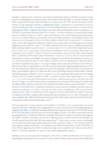
               NdCl -treated CdS thin film is shown in Figure 1A. In this work, “W/O Nd” denotes the absence of Nd,
                   3
               whereas “W Nd” represents its presence. Supplementary Figure 1 presents the J-V characteristics of devices
               treated with different NdCl  concentrations, and the detailed photovoltaic parameters are summarized in
                                       3
               Supplementary Table 1. Supplementary Figure 2 shows the statistical distribution of device performance. As
               the NdCl  concentration increases from 0 to 0.05 mol L , the device efficiency increases progressively;
                                                                -1
                       3
               however, a further increase to 0.1 mol L  reduces the efficiency. The overall improvement in photovoltaic
                                                 -1
               metrics is ascribed to enhanced crystallinity and preferential orientation, reduced defect density, and
               improved carrier transport in Sb Se  thin films enabled by effective Nd incorporation . As shown in
                                                                                            [24]
                                               3
                                            2
               Figure 1B, the XRD patterns of CdS films exhibit characteristic peaks corresponding to the standard
               hexagonal structure (PDF#41-1049) [25,26] . No shift is observed in the (100) and (101) diffraction planes after
               NdCl  treatment, likely because the ionic (1.10 Å) and covalent (1.60 Å) radii of Nd are larger than those of
                   3
               Cd (0.97 and 1.44 Å, respectively), which hinders Nd diffusion into the CdS lattice and results in its
               localization on the surface . Figure 1C shows the transmittance spectra of both films, indicating that
                                      [27]
               NdCl -treated CdS exhibits higher optical transmittance across 300-1,100 nm, with the most pronounced
                   3
               enhancement at shorter wavelengths. The optical bandgaps estimated from the transmittance spectra are
               2.31 eV for untreated CdS and 2.38 eV for NdCl -treated CdS. The corresponding Tauc plots for CdS are
                                                         3
               provided in Supplementary Figure 3. The larger bandgap reduces parasitic absorption in the CdS layer,
               allowing more high-energy photons to reach the absorber and thereby supporting higher photocurrent .
                                                                                                        [27]
               XPS was subsequently employed to analyze the elemental migration and chemical states of untreated and
               NdCl -treated samples. Figure 1D-F shows the XPS spectra of CdS films with and without NdCl  treatment,
                                                                                                 3
                   3
               with binding energies calibrated to the C 1s peak at 285 eV. No significant shift is observed in the binding
               energies of the Cd 3d and S 2p peaks. For NdCl -treated CdS, distinct Nd 3d peaks appear at 977.57 and
                                                         3
               1,011.91 eV, with a possible Nd-O peak between them, confirming the presence of Nd on the CdS
               surface [28,29] . Figure 1G and H presents surface scanning electron microscopy (SEM) images of CdS films with
               and without NdCl  treatment, respectively. The untreated CdS surface contains numerous particles [30,31] , while
                              3
               the NdCl -treated film shows a significant reduction in surface particles, yielding a smoother and more
                       3
               uniform morphology. To further verify the smoother surface morphology, AFM was performed.
               Supplementary Figure 4A and B shows AFM images of CdS films with and without NdCl  treatment,
                                                                                                3
               revealing reduced surface roughness after treatment (Ra decreased from 26.8 to 23.6 nm). The smoother CdS
               surface obtained after NdCl  treatment promotes the growth of Sb Se  grains, thereby improving CdS/ Sb Se 3
                                                                                                       2
                                      3
                                                                       2
                                                                         3
               heterojunction quality and reducing leakage current .
                                                          [32]
               TAS was employed to measure minority carrier lifetime in CdS films. A 400 nm pulsed laser was used to
               excite the CdS surface, with delay times ranging from 0 to 6,000 ps. As shown in the TAS mapping images in
               Supplementary Figure 5A and B, the maximum absorption peak appears at 488 nm for W/O Nd and 502 nm
               for W Nd, indicating a red shift associated with bandgap variation. This shift is consistent with the
               morphology results, as SEM and AFM show markedly reduced particle features and decreased roughness
               after NdCl  treatment, which lowers the spectral weighting of particle-related contributions and shifts the
                        3
               overall response toward the bulk CdS band-edge position . Carrier decay curves at various wavelengths
                                                                 [33]
               were extracted and fitted using a double-exponential model, as shown in Figure 1I. The relevant calculations
               are provided in Supplementary Note 1. The minority carrier lifetime increases from 78 ps for W/O Nd to 129
               ps for W Nd, suggesting that NdCl  treatment prolongs carrier migration and reduces surface defect
                                              3
               density . Delay time-dependent TA spectra are provided in Supplementary Figure 6.
                     [34]

               Building on the previous systematic investigation of the effects of NdCl  modification on the structural,
                                                                              3
               morphological, and optoelectronic properties of CdS, we further explore whether and how this modification

