
Page 94 - Read Online
P. 94
Page 18 of 31 Kim et al. Soft Sci 2024;4:33 https://dx.doi.org/10.20517/ss.2024.28
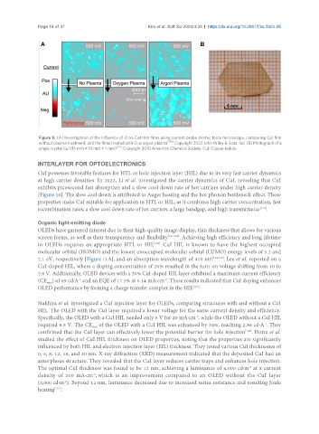
Figure 9. (A) Investigation of the influence of O on CuI thin films using current probe atomic force microscopy, comparing CuI film
without plasma treatment, and the films treated with O or argon plasma [119] . Copyright 2023 John Wiley & Sons, Inc; (B) Photograph of a
single crystal CuI (15 mm × 10 mm × 1 mm) [32] . Copyright 2010 American Chemical Society. CuI: Copper iodide.
INTERLAYER FOR OPTOELECTRONICS
CuI possesses favorable features for HTL or hole injection layer (HIL) due to its very fast carrier dynamics
at high carrier densities. In 2022, Li et al. investigated the carrier dynamics of CuI, revealing that CuI
exhibits picosecond fast absorption and a slow cool down rate of hot carriers under high carrier density
[Figure 10]. The slow cool down is attributed to Auger heating and the hot phonon bottleneck effect. These
properties make CuI suitable for application in HTL or HIL, as it combines high carrier concentration, fast
[120]
recombination rates, a slow cool down rate of hot carriers, a large bandgap, and high transmittance .
Organic light-emitting diode
OLEDs have garnered interest due to their high-quality image display, thin thickness that allows for various
screen forms, as well as their transparency and flexibility [121,122] . Achieving high efficiency and long lifetime
in OLEDs requires an appropriate HTL or HIL . CuI HIL is known to have the highest occupied
[123]
molecular orbital (HOMO) and the lowest unoccupied molecular orbital (LUMO) energy levels of 5.2 and
2.1 eV, respectively [Figure 11A], and an absorption wavelength of 410 nm [124,125] . Lee et al. reported on a
CuI-doped HIL, where a doping concentration of 20% resulted in the turn-on voltage shifting from 10 to
2.9 V. Additionally, OLED devices with a 20% CuI-doped HIL layer exhibited a maximum current efficiency
-2
-1
(CE ) of 69 cd·A and an EQE of 17.5% at 0.14 mA·cm . These results indicated that CuI doping enhances
max
OLED performance by forming a charge transfer complex in the HIL .
[126]
Stakhira et al. investigated a CuI injection layer for OLEDs, comparing structures with and without a CuI
HIL. The OLED with the CuI layer required a lower voltage for the same current density and efficiency.
-2
Specifically, the OLED with a CuI HIL needed only 6 V for 20 mA·cm , while the OLED without a CuI HIL
required 8.5 V. The CE of the OLED with a CuI HIL was enhanced by 34%, reaching 2.86 cd·A . They
-1
max
[124]
confirmed that the CuI layer can effectively lower the potential barrier for hole injection . Hotra et al.
studied the effect of CuI HIL thickness on OLED properties, noting that the properties are significantly
influenced by both HIL and electron injection layer (EIL) thickness. They tested various CuI thicknesses of
0, 5, 8, 12, 18, and 30 nm. X-ray diffraction (XRD) measurement indicated that the deposited CuI had an
amorphous structure. They revealed that the CuI layer reduces carrier traps and enhances hole injection.
The optimal CuI thickness was found to be 12 nm, achieving a luminance of 4,000 cd·m at a current
-2
density of 200 mA·cm , which is an improvement compared to an OLED without the CuI layer
-2
-2
(3,000 cd·m ). Beyond 12 nm, luminance decreased due to increased series resistance and resulting Joule
[127]
heating .