
Page 91 - Read Online
P. 91
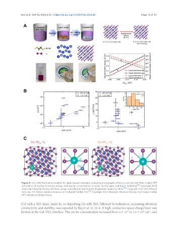
Kim et al. Soft Sci 2024;4:33  https://dx.doi.org/10.20517/ss.2024.28           Page 15 of 31


                Figure 6. (A) (left) Fabrication method for sulfur-doped iodination, including photographs of the Cu and CuI thin films. (right) DFT
                                                                                            [28]
                calculation of doping formation energy and doping concentration of sulfur during vapor and liquid  iodination  . Copyright 2022
                                                                                   [109]
                American Chemical Society; (B) Hole carrier concentration and mobility of selenium-doped CuI films  . Copyright 2021 John Wiley &
                                                            [110]
                Sons, Inc; (C) Defect complex structure of Cs-doped CuI thin film  . Copyright 2022 American Chemical Society. CuI: Copper iodide;
                DFT: density functional theory.
               CuI with a TiO  layer, made by co-depositing Cu with TiO  followed by iodination, increasing electrical
                                                                   2
                             2
               conductivity and stability, was reported by Raj et al. in 2019. A high conductive space-charge layer was
               formed at the CuI-TiO  interface. The carrier concentration increased from 4 × 10  to 1.3 × 10  cm , and
                                                                                                20
                                                                                                     -3
                                                                                      19
                                   2