
Page 87 - Read Online
P. 87
Kim et al. Soft Sci 2024;4:32 https://dx.doi.org/10.20517/ss.2024.28 Page 11 of 31
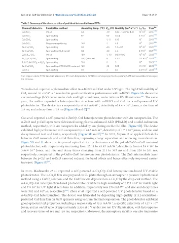
Table 2. Summary of the characteristics of published data on CuI-based TFTs
-1
-1
2
Channel/dielectric Fabrication method Annealing temp. (°C) V (V) Mobility (cm ·V ·s ) I on /I off Year Ref.
DS
1
CuI/SiO 2 Ink-jet 60 -40 1.86 ± 1.6 (max 4.4) 10 -10 2 2016 [44]
2 [42]
CuI/SiO Spin-coating RT -50 0.44 5 × 10 2018
2
2 [42]
CuI/ZrO Spin-coating - -1, -5 1.93 10 2018
2
CuI/SiO 2 Magnetron sputtering 140 -1 4.8 10 2 2019 [89]
6 7 [80]
Zn-CuI/SiO Spin-coating 80 -40 5.3 ± 0.5 10 -10 2020
2
Zn-CuI/SiO 2 Spin-coating (O treated) 80 -40 4.4 8 × 10 6 2021 [90]
2
3 5 [81]
CuBr I /SiO Ink-jet 150 -1, -10 0.02-9.06 10 -10 2022
x 1-x 2
4 [40]
Al O /CuI/SiO 2 Spin-coating 300 (vacuum) -5 4.02 1.12 × 10 2022
3
2
Su8/CuBrI/SiO + Al O Spin-coating 100 -1 5 10 4 2023 [83]
2
3
2
7 [91]
Zn-CuI/SiO Spin-coating APTES SAM treatment 120 -30 1.24 1.1 × 10 2023
2
CuI/CS Spin-coating RT -1 60 6.6 × 10 3 2023 [84]
CuI: Copper iodide; TFTs: thin-film transistors; RT: room temperature; APTES: (3-aminopropyl)triethoxysilane; SAM: self-assembled monolayer;
CS: chitosan.
Yamada et al. reported a photovoltaic effect in a-IGZO and CuI under UV light. The high Hall mobility of
CuI, around 20 cm ·V ·s , resulted in good rectification performance with a-IGZO. Figure 5A shows the
-1 -1
2
current-voltage (I-V) curve under dark and light conditions, under 365 nm UV illumination . The same
[64]
year, the author reported a heterojunction structure with a-IGZO and CuI for a self-powered UV
11
-1
photodetector. The device has a responsivity of 0.6 mA·W , detectivity of 8.4 × 10 Jones, a rise time of
[94]
2.5 ms, and a decay time of 35 ms [Figure 5B and C] .
Cao et al. reported a self-powered n-ZnO/p-CuI heterojunction photodetector with Au nanoparticles. The
n-ZnO and p-CuI layers were fabricated using plasma-enhanced ALD (PEALD) and a solid-iodination
method, respectively, with Au nanoparticles added by ion plating on the CuI film [Figure 5D]. The device
-1
10
exhibited high performance with a responsivity of 61.5 mA·W , detectivity of 1.7 × 10 Jones, and rise and
decay times of 0.41 and 0.08 s, respectively [Figure 5E and F] . In 2023, Shyam et al. applied ZnS shells
[96]
between ZnO nanorods and a CuI thin film, improving charge separation and reducing recombination.
Figure 5G and H show the improved optoelectrical performances of the p-CuI/ZnS/n-ZnO nanorod
photodetector, with responsivity increasing from 25.11 to 43.85 mA·W , detectivity from 4.59 × 10 to
13
-1
3.84 × 10 Jones, and rise and decay times changing from 211 to 305 ms and from 220 to 261 ms,
14
respectively, compared to the p-CuI/n-ZnO heterojunction photodetector. The ZnS intermediate layer
between the p-CuI and n-ZnO nanorod reduced the band offsets and hence effectively improved carrier
transport [Figure 5I] .
[99]
In 2019, Madusanka et al. reported a self-powered n-Cu O/p-CuI heterojunction-based UV-visible
2
photodetector. The n-Cu O film was prepared on Cu plates through an atmospheric pressure hydrothermal
2
method using a CuSO solution, and the CuI film was deposited on n-Cu O by the drop-cast method. The
4
2
n-Cu O/p-CuI heterojunction-based photodetector exhibited a high sensitivity of 2.355 × 10 for visible light
5
2
and 7 × 10 for UV light at zero bias. In addition, responsivity was 250 mA·W and rise and decay times
-1
3
were 582 and 817 μs, respectively . Zhou et al. reported a self-powered UV photodetector based on a
[100]
n-GaN/p-CuI heterojunction. The device was fabricated by depositing high-quality [111] orientation-
preferred CuI thin film on GaN epilayers using vacuum thermal evaporation. The photodetector exhibited
good optoelectrical properties, including a responsivity of 75.5 mA·W , a specific detectivity of 1.27 × 10
-1
12
Jones, and an on/off ratio of approximately 2,320 at 0 V under 360 nm UV illumination, with fast response
and recovery times of 160 and 158 ms, respectively. Moreover, the atmosphere stability was also impressive