
Page 83 - Read Online
P. 83
Kim et al. Soft Sci 2024;4:33 https://dx.doi.org/10.20517/ss.2024.28 Page 7 of 31
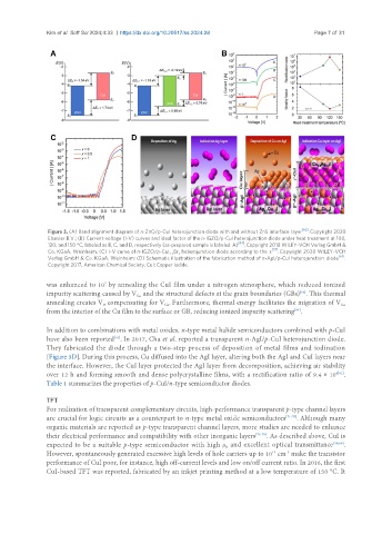
Figure 3. (A) Band alignment diagram of n-ZnO/p-CuI heterojunction diode with and without ZnS interface layer [62] . Copyright 2020
Elsevier B.V.; (B) Current-voltage (I-V) curves and ideal factor of the n-IGZO/p-CuI heterojunction diode under heat treatment at 100,
120, and 150 °C, labeled as B, C, and D, respectively (as-prepared sample is labeled A) [64] . Copyright 2018 WILEY-VCH Verlag GmbH &
Co. KGaA, Weinheim; (C) I-V curve of n-IGZO/p-CuI Br heterojunction diode according to the x [57] . Copyright 2020 WILEY-VCH
1-x x
Verlag GmbH & Co. KGaA, Weinheim; (D) Schematic illustration of the fabrication method of n-AgI/p-CuI heterojunction diode [61] .
Copyright 2017, American Chemical Society. CuI: Copper iodide.
was enhanced to 10 by annealing the CuI film under a nitrogen atmosphere, which reduced ionized
7
impurity scattering caused by V and the structural defects at the grain boundaries (GBs) . This thermal
[65]
Cu
annealing creates V , compensating for V . Furthermore, thermal energy facilitates the migration of V Cu
I
Cu
from the interior of the Cu film to the surface or GB, reducing ionized impurity scattering .
[64]
In addition to combinations with metal oxides, n-type metal halide semiconductors combined with p-CuI
have also been reported . In 2017, Cha et al. reported a transparent n-AgI/p-CuI heterojunction diode.
[61]
They fabricated the diode through a two-step process of deposition of metal films and iodination
[Figure 3D]. During this process, Cu diffused into the AgI layer, altering both the AgI and CuI layers near
the interface. However, the CuI layer protected the AgI layer from decomposition, achieving air stability
over 12 h and forming smooth and dense polycrystalline films, with a rectification ratio of 9.4 × 10 .
4[61]
Table 1 summarizes the properties of p-CuI/n-type semiconductor diodes.
TFT
For realization of transparent complementary circuits, high-performance transparent p-type channel layers
are crucial for logic circuits as a counterpart to n-type metal oxide semiconductors [71-75] . Although many
organic materials are reported as p-type transparent channel layers, more studies are needed to enhance
their electrical performance and compatibility with other inorganic layers [76-79] . As described above, CuI is
expected to be a suitable p-type semiconductor with high μ and excellent optical transmittance [38,66] .
h
-3
However, spontaneously generated excessive high levels of hole carriers up to 10 cm make the transistor
19
performance of CuI poor, for instance, high off-current levels and low on/off current ratio. In 2016, the first
CuI-based TFT was reported, fabricated by an inkjet printing method at a low temperature of 150 °C. It