
Page 84 - Read Online
P. 84
Page 8 of 31 Kim et al. Soft Sci 2024;4:33 https://dx.doi.org/10.20517/ss.2024.28
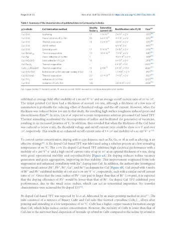
Table 1. Summary of the characteristics of published data on CuI-based p/n diodes
Ideality Saturation Ref.
p/n-diode CuI fabrication method Rectification ratio IF/IR Year
factor η current (A)
-11 7 [66]
CuI/ZnO Sputtering 1.7 1.3 × 10 2 × 10 , ± 2 V 2013
-15 7 [66]
CuI/ZnO Vapor iodization of Cu film 1.6 6.2 × 10 4 × 10 , ± 2 V 2013
7
CuI/ZnO Thermal evaporation 1.8 3.2 × 10 -13 2 × 10 , ± 2 V 2013 [66]
2 [67]
CuI/ZnO SILAR method - - 6 × 10 , 3 V 2015
9
CuI/ZnO Epitaxial growth 1.7 1.1 × 10 -12 2 × 10 , ± 2 V 2016 [59]
5
CuI/BaSnO 3-δ Thermal evaporation 1.5 9.9 × 10 -13 7 × 10 , ± 2 V 2017 [63]
4
CuI/AgI Vapor iodization of Cu film 1 - 9.4 × 10 , ± 2 V 2017 [61]
6 [64]
CuI/InGaZnO Solid iodination of Cu N 1.6 - 6 × 10 , ± 2 V 2018
3
3 [68]
CuI/Ga O 3 Thermal evaporation - - 6 × 10 , ± 2 V 2020
2
9
CuBr I /InGaZnO Thermal evaporation 1.9 2 × 10 -12 2 × 10 , ± 1.5 V 2020 [57]
1-x x
7 [62]
CuI/ZnS/ZnO Iodination of Cu film and spin-coating of CuI 1.1 - 1.7 × 10 , ± 2 V 2021
-16 7 [65]
CuI/SiZnSnO Thermal evaporation 2.7 0.7 × 10 7 × 10 , ± 2 V 2021
CuI/TiO 2 Iodination of CuO film 4.4 - - 2023 [69]
5 [70]
CuI/ZnO Iodination of CuN film 1.22 - 1.05 × 10 , ± 2 V 2024
3
CuI: Copper iodide; IF: forward current; IR: reverse current; SILAR: successive ionic layer absorption and reaction.
exhibited an average field-effect mobility of 1.86 cm ·V ·s and an average on/off current ratio of 10 to 10 .
2
2
-1 -1
1
The inkjet printed CuI layer had a thickness of around 100 nm, although a thickness of a few tens of
nanometers is preferable for reducing offset of threshold voltage and the off-current. However, when the
thickness was reduced below 100 nm in that study, the resulting high surface roughness induced pores and
discontinuous films . In 2018, Liu et al. reported a room-temperature solution-processed CuI-based TFT.
[44]
Thermal annealing accelerated the decomposition of iodine and facilitated the generation of vacancies,
resulting in an increased presence of V . In addition, they revealed that when the thickness of the CuI layer
I
was reduced to below 8 nm, the threshold voltage and on/off current ratio could be close to 0 V and over
2
10 , respectively. This results in an enhanced on/off current ratio of 5 × 10 and mobility of 0.44 cm ·V ·s .
2
-1 -1[42]
2
To control carrier concentration, doping with n-type dopants, such as Zn, Ga, or Al as well as alloying, is an
[80]
effective strategy . A Zn-doped CuI-based TFT was fabricated using a solution process at a low annealing
temperature of 80 °C. The 2.5% Zn-doped CuI-based TFT exhibited high electrical performance with a
2
7
-1 -1
mobility of 5 cm ·V ·s and a high on/off current ratio of up to 10 at an optimal thickness of 9 nm, along
with good operational stability and reproducibility [Figure 4A]. Zn doping reduces iodine vacancy
generation and grain aggregation, improving its bias stability. This improvement originated from hole
suppression and enhanced crystallinity with Zn doping into CuI. In addition, the authors also investigated
2+
various metal cations (Ni , Pb , Bi , Ga , and Sn ) as dopants for CuI [Figure 4B]. CuI doped with 5 mol%
2+
2+
3+
4+
3+
2+
3+
of Bi and Pb exhibited mobility of 0.45 and 0.34 cm ·V ·s , respectively, each with a similar on/off current
2
-1 -1
ratio of 10 . Given that the ionic radius of Pb (120 pm) is larger than that of Bi (108 pm), it is expected
2+
4
3+
that the doping efficiency of Pb would be lower than that of Bi . Ga-doped CuI TFT exhibited poor
3+
2+
performance, due to the small ionic radius, which can act as interstitial impurities. No transfer
characteristics were achieved for Ni-doped TFT .
[80]
[81]
Br-doped CuI-based TFT was reported by Li et al., fabricated by an inkjet printing method in 2022 . The
inks consisted of a mixture of binary CuBr and CuI salts that formed crystalline CuBr I alloys after
x 1-x
printing and annealing at a low temperature of 60 °C. CuBr has a higher copper vacancy formation energy
than CuI, which helps reduce carrier concentration. However, the mobility of CuBr is lower than that of
CuI due to the narrower band dispersion of bromide 4p orbital in CuBr compared to the iodine 5p orbital in