
Page 195 - Read Online
P. 195
Jeon et al. Soft Sci. 2025, 5, 1 https://dx.doi.org/10.20517/ss.2024.35 Page 25 of 39
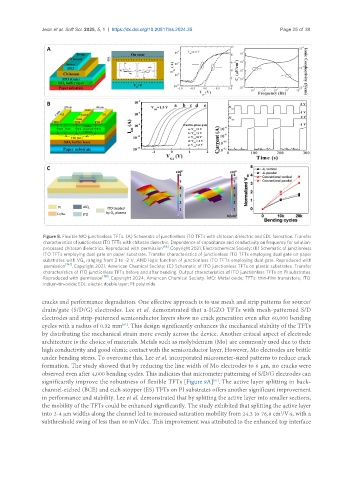
Figure 8. Flexible MO junctionless TFTs. (A) Schematic of junctionless ITO TFTs with chitosan dielectric and EDL formation. Transfer
characteristics of junctionless ITO TFTs with chitosan dielectric. Dependence of capacitance and conductivity on frequency for solution-
[66]
processed chitosan dielectrics. Reproduced with permission . Copyright 2021, Electrochemical Society; (B) Schematic of junctionless
ITO TFTs employing dual gate on paper substrate. Transfer characteristics of junctionless ITO TFTs employing dual gate on paper
substrates with VG ranging from 2 to -2 V. AND logic function of junctionless ITO TFTs employing dual gate. Reproduced with
3
permission [194] . Copyright 2021, American Chemical Society; (C) Schematic of ITO junctionless TFTs on plastic substrates. Transfer
characteristics of ITO junctionless TFTs before and after bending. Output characteristics of ITO junctionless TFTs on PI substrates.
Reproduced with permission [198] . Copyright 2024, American Chemical Society. MO: Metal oxide; TFTs: thin-film transistors; ITO:
indium-tin-oxide; EDL: electric double layer; PI: polyimide.
cracks and performance degradation. One effective approach is to use mesh and strip patterns for source/
drain/gate (S/D/G) electrodes. Lee et al. demonstrated that a-IGZO TFTs with mesh-patterned S/D
electrodes and strip-patterned semiconductor layers show no crack generation even after 60,000 bending
cycles with a radius of 0.32 mm . This design significantly enhances the mechanical stability of the TFTs
[61]
by distributing the mechanical strain more evenly across the device. Another critical aspect of electrode
architecture is the choice of materials. Metals such as molybdenum (Mo) are commonly used due to their
high conductivity and good ohmic contact with the semiconductor layer. However, Mo electrodes are brittle
under bending stress. To overcome this, Lee et al. incorporated micrometer-sized patterns to reduce crack
formation. The study showed that by reducing the line width of Mo electrodes to 6 µm, no cracks were
observed even after 4,000 bending cycles. This indicates that micrometer patterning of S/D/G electrodes can
significantly improve the robustness of flexible TFTs [Figure 9A] . The active layer splitting in back-
[61]
channel-etched (BCE) and etch-stopper (ES) TFTs on PI substrates offers another significant improvement
in performance and stability. Lee et al. demonstrated that by splitting the active layer into smaller sections,
the mobility of the TFTs could be enhanced significantly. The study exhibited that splitting the active layer
2
into 2-4 μm widths along the channel led to increased saturation mobility from 24.3 to 76.8 cm /V·s, with a
subthreshold swing of less than 80 mV/dec. This improvement was attributed to the enhanced top interface