
Page 192 - Read Online
P. 192
Page 22 of 39 Jeon et al. Soft Sci. 2025, 5, 1 https://dx.doi.org/10.20517/ss.2024.35
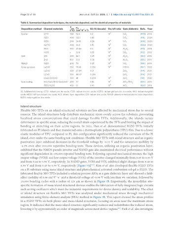
Table 6. Summarized deposition techniques, the materials deposited, and the electrical properties of materials
T μ
Deposition method Channel materials max FE 2 -1 -1 SS (V/decade) On/off ratio Gate dielectric Refs. Year
(°C) (cm ·V ·s )
8
Sputter IZTO 380 52.4 0.2 10 SiO [178] 2014
2
ITZO 400 122.1 0.18 - SiO 2 [118] 2024
8
ITZO 290 26.15 0.26 10 SiO [108] 2024
2
IGZTO 400 26.8 0.15 10 8 SiO 2 [126] 2020
6
IWO 300 25.86 0.3 10 Al O [111] 2018
2 3
6
HIZO - 32.6 0.55 10 SiO 2 [112] 2012
ALD IZO 200 42.1 0.29 10 9 Al O 3 [134] 2016
2
7
ZnO 100 37.1 0.38 10 Al O 3 [135] 2019
2
PEALD IGZO 200 70 0.25 10 8 SiO 2 [136] 2019
8
Spray pyrolysis LaZnO 250 19.06 0.256 10 HfZrO [127] 2023
LaZnO 350 27.84 0.21 - ZrO x [114] 2021
LiZnO 350 48.47 0.256 - ZrO [114] 2021
x
(GaO/ZnO)×3 350 41 0.209 10 8 ZrO x [98] 2022
4
Spin coating InO/GaO/ZnO/GaO/InO 200 37 0.16 10 AlO /ZrO [125] 2015
x 2
8
ITZO/IGZO 450 51 0.41 10 AlO x [100] 2018
SS: Subthreshold swing; IZTO: indium zinc tin oxide; ITZO: indium tin zinc oxide; IGZTO: indium gallium zinc tin oxide; IWO: indium tungsten
oxide; HIZO: hafnium indium zinc oxide; ALD: atomic layer deposition; IZO: indium zinc oxide; PEALD: plasma-enhanced atomic layer deposition;
IGZO: indium gallium zinc oxide.
Island structure
Flexible MO TFTs on an island-structured substrate are less affected by mechanical stress due to several
reasons. The island structures help distribute mechanical stress evenly across the substrate, preventing
localized stress concentrations that could damage flexible TFTs. Additionally, the islands isolate
deformation to specific areas, reducing the overall strain experienced by the TFTs and limiting the impact of
bending or stretching on their active regions. In 2021, Han et al. demonstrated IGZO TFTs initially
fabricated on PI islands and then transferred onto a thermoplastic polyurethane (TPU) film. Due to a lower
elastic modulus of TPU compared to PI, this configuration significantly reduced the curvature of the PI
island, even under the same bending test conditions. Flexible MO TFTs with island structure and an organic
passivation layer exhibited decreases in the threshold voltage by -0.22 V and the saturation mobility by
-2.3% even after 250,000 repetitive bending tests. These devices, utilizing an organic passivation layer,
exhibited that the NMOS pseudo inverter and NAND gate also maintained electrical performance without
significant degradation in 100,000 repeated bending tests. Following repeated mechanical stresses, the high
output voltage (VOH) and low output voltage (VOL) of the inverter changed minimally from 8.85 to 8.93 V
and from 0.44 to 0.50 V, respectively. In NAND gates, VOH and VOL exhibited slight changes from 8.46 to
8.56 V and from 0.45 to 0.55 V, respectively [Figure 7A] . Kim et al. also developed flexible IGZO TFTs
[102]
on a PI substrate using mesa island structure and photochemical activated combustion sol-gel a-IGZO. The
fabricated flexible MO TFTs included a solution process AlOx as a gate dielectric layer and showed a field-
effect mobility of 6.06 cm ·V ·s and a threshold voltage of -0.99 V with less than 9% variation, followed by
2
-1 -1
10,000 bending cycles with a radius of 125 μm as shown in Figure 7B. Importantly, the monolithic site-
specific formation of mesa island structured devices enables the fabrication of fully integrated logic circuits
such as ring oscillators which meet the industrial requirements for device density and scalability. The effect
of island structure on flexible MO TFTs was analyzed under mechanical stress through mechanical
simulation using finite-element analysis (FEA) method in Figure 7B. This report showed the stress profiles
in a-IGZO TFTs on both planar and mesa island structures, focusing on areas near the maximum stress
region. It indicated that the mesa island structure significantly reduces and redistributes the induced stress,
[33]
lowering it by approximately an order of magnitude across most device regions . Park et al. also investigate