
Page 189 - Read Online
P. 189
Jeon et al. Soft Sci. 2025, 5, 1 https://dx.doi.org/10.20517/ss.2024.35 Page 19 of 39
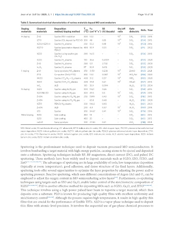
Table 5. Summarized electrical characteristics of various materials dopped MO semiconductors
Doping Channel Deposition T max μ FE SS On/off Gate
-1
-1
materials materials method/doping method (°C) (cm ·V ·s ) (V/decade) ratio dielectric Refs. Year
2
H doping ZnO Sputter/UV irradiation 300 14.2 - 10 6 SiN x [151] 2018
10
IZTO Sputter/ESL deposit by PECVD 350 48 0.15 10 SiO [154] 2015
2
IGZO/IGZO:H Sputter/H plasma 250 55.3 0.18 10 8 SiO 2 [153] 2016
2
IGZTO Sputter/passivation deposit by 400 85.9 0.33 - SiO [59] 2022
2
PEALD
IGZO Sputter/using sputter gas 200 16.15 - - SiO [156] 2018
2
(Ar/H )
2
IGZO Sputter/H plasma 150 36.6 0.4559 - SiO [155] 2020
2 2
ZnO Sputter/H plasma 200 12.1 2.702 - SiO 2 [155] 2020
2
In O 3 Sputter/H plasma RT 55.9 1.435 - SiO 2 [155] 2020
2
2
8
F doping ZnO Spray pyrolysis/NF plasma 350 31.59 0.238 10 ZrAlO [163] 2021
3
ZTO Co-sputter (ZnO/FTO) 350 14.2 0.087 10 9 AlO :Nd [166] 2023
x
6
IWZO Sputter/CF /N + O plasma 400 31.2 0.37 10 HfO [165] 2020
4 2 2 2
IGZO Sputter/CHF /O plasma 400 39.8 0.21 10 6 HfLaO [167] 2014
3
2
InO ALD 150 35.9 0.094 - Al O [173] 2024
x 2 3
N doping IGZO Sputter using Ar,N gas 300 19.21 0.26 - SiO 2 [158] 2016
2
7
IGZO:N/IZO Sputter using Ar,N gas 300 49.6 0.5 10 SiO [159] 2016
2 2
8
ZnON Sputter using Ar/O /N gas 250 51.99 0.42 10 SiO 2 [110] 2015
2
2
ZnON Sputter using Ar/O /N gas - 65.8 0.48 - Al O [113] 2020
2 2 2 3
IGZO PEALD/N plasma 350 106.5 0.113 - Al O 3 [161] 2023
2
2
ZnON ALD 250 4.8 0.47 10 7 Al O 3 [160] 2018
2
9
IZO Sputter 350 24.67 0.41 10 SiO 2 [176] 2016
Metal doping IBZO Spin coating 450 18 - - SiO 2 [60] 2013
ISZO Spin coating 450 25 - - SiO [60] 2013
2
LaZnO Spray pyrolysis 350 27.84 0.21 - ZrO x [114] 2021
MO: Metal oxide; SS: subthreshold swing; UV: ultraviolet; IZTO: indium zinc tin oxide; ESL: etch stopper layer; PECVD: plasma-enhanced chemical
vapor deposition; IGZO: indium gallium zinc oxide; IGZTO: indium gallium zinc tin oxide; PEALD: plasma-enhanced atomic layer deposition; ZTO:
zinc tin oxide; FTO: fluorine tin oxide; IWZO: indium tugsten zinc oxide; IZO: indium zinc oxide; ALD: atomic layer deposition; IBZO: indium
barium zinc oxide; ISZO: indium strontium zinc oxide.
Sputtering is the predominant technique used to deposit vacuum-processed MO semiconductors. It
involves bombarding a target material with high-energy particles, causing atoms to be ejected and deposited
onto a substrate. Sputtering techniques include RF, RF-magnetron, direct current (DC), and pulsed DC
sputtering. These methods have been widely used to deposit materials such as IGZO, IZO, ITZO, and
ZnO [111-113,118,126,178] . The advantages of sputtering are its large availability of tools, low-temperature deposition
(typically at room temperature), good adhesion, and dense structure of the final layers. Additionally,
sputtering tools offer several opportunities to optimize the layer properties by adjusting the power and/or
sputtering pressure. Reactive sputtering, which uses different concentrations of Argon (Ar) and O , can be
2
employed to adjust the oxygen content in MO semiconducting active layers . Furthermore, co-sputtering
[179]
techniques using targets such as IZO and Ga O enable better control of the stoichiometric composition of
3
2
IGZO [10,12,94,179] . PLD is another effective method for depositing MOs such as IGZO, Ga O and ZITO [92,148,180] .
2
3
This technique involves using a high-power pulsed laser beam to vaporize a target material, which then
deposits onto a substrate. PLD is known for producing high-quality films with excellent uniformity and
stoichiometry control [181,182] . Although the process requires high temperatures, it results in high-quality thin
films that are crucial for the performance of flexible TFTs. ALD is a vapor-phase technique used to deposit
thin films with atomic-level precision. It involves the sequential use of gas-phase chemical processes to