
Page 186 - Read Online
P. 186
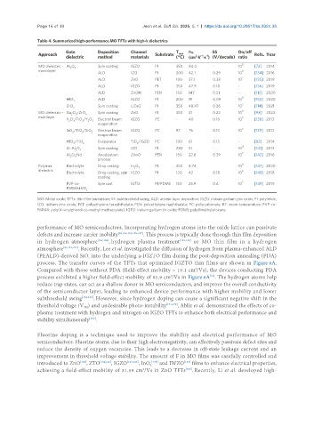
Page 16 of 39                           Jeon et al. Soft Sci. 2025, 5, 1  https://dx.doi.org/10.20517/ss.2024.35

               Table 4. Summarized high-performance MO TFTs with high-k dielectrics

                          Gate        Deposition   Channel          T    μ FE    SS        On/off
                Approach                                    Substrate  max  2  -1  -1            Refs. Year
                          dielectric  method       materials        (°C) (cm ·V ·s ) (V/decade) ratio
                MO dielectric -   Al O 3  Spin coating  IGZO  PI    350  84.4     -        10 5  [72]  2014
                            2
                monolayer                                                                    9
                                      ALD          IZO      PI      200  42.1     0.29     10    [134] 2016
                                      ALD          ZnO      PET     100  37.1     0.38     10 7  [135] 2019
                                      ALD          IGZO     PI      350  47.9     0.18     -     [136] 2019
                                      ALD          ZnON     PEN     150  147      0.21     -     [113] 2020
                                                                                             11
                          HfO         ALD          IGZO     PI      200  19       0.09     10    [150] 2020
                             2
                                                                                             7
                          ZrO x       Spin coating  LiZnO   PI      350  48.47    0.26     10    [114] 2021
                                                                                             8
                MO dielectric -   Ga O /ZrO  Spin coating  ZnO  PI  350  41       0.22     10    [98]  2022
                            2  3  x
                multilayer                                                                   5
                          Y O /TiO /Y O 3  Electron beam   IGZO  PC  -   40       0.16     10    [138] 2013
                           2
                             3
                                2
                                  2
                                      evaporation
                                                                                             5
                          SiO /TiO /SiO  Electron beam   IGZO  PC   RT   76       0.13     10    [139] 2013
                            2   2   2
                                      evaporation
                          HfO /TiO    Evaporator   TiO /IGZO  PC    100  61       0.13     -     [82]  2014
                             2  2                    x
                          Zr-Al O 3   Spin coating  IZO     PI      280  51       -        10 4  [141] 2013
                              2
                                                                                             7
                          Al O :Nd    Anodization   ZrInO   PEN     150  22.6     0.39     10    [142] 2016
                            2  3
                                      process
                                                                                             6
                Polymer   Electrolyte  Drop casting  In O   PI      250  8.74              10    [147] 2020
                                                    2  3
                dielectric                                                                   6
                          Electrolyte  Drop casting, spin  IGZO  PI  120  42      0.18     10    [148] 2018
                                      coating
                                                                                             7
                          PVP-co-     Spin cast    IGTO     PI/PDMS  150  25.9    0.4      10    [149] 2019
                          PMMA:HfO x
               MO: Metal oxide; TFTs: thin-film transistors; SS: subthreshold swing; ALD: atomic layer deposition; IGZO: indium gallium zinc oxide; PI: polyimide;
               IZO: indium zinc oxide; PET: polyethylene terephthalate; PEN: polyethylene naphthalate; PC: polycarbonate; RT: room temperature; PVP-co-
               PMMA: poly(4-vinylphenol-co-methyl methacrylate); IGTO: indium gallium tin oxide; PDMS: polydimethylsiloxane.
               performance of MO semiconductors. Incorporating hydrogen atoms into the oxide lattice can passivate
               defects and increase carrier mobility [59,152,153,155-157] . This process is typically done through thin film deposition
               in  hydrogen  atmosphere [152,156] , hydrogen  plasma  treatment [153,155]   or  MO  thin  film  in  a  hydrogen
               atmosphere [59,151,154] . Recently, Lee et al. investigated the diffusion of hydrogen from plasma-enhanced ALD
               (PEALD)-derived SiO  into the underlying a-IGZTO film during the post-deposition annealing (PDA)
                                  2
               process. The transfer curves of the TFTs that optimized IGZTO thin films are shown in Figure 6A.
               Compared with those without PDA (field-effect mobility = 19.1 cm /Vs), the devices conducting PDA
                                                                           2
                                                                  2
               process exhibited a higher field-effect mobility of 85.9 cm /Vs in Figure 6A . The hydrogen atoms help
                                                                                 [59]
               reduce trap states, can act as a shallow donor in MO semiconductors, and improve the overall conductivity
               of the semiconductor layer, leading to enhanced device performance with higher mobility and lower
               subthreshold swing [169,170] . However, since hydrogen doping can cause a significant negative shift in the
               threshold voltage (V ) and undesirable photo-instability [171,172] , Abliz et al. demonstrated the effects of co-
                                 TH
               plasma treatment with hydrogen and nitrogen on IGZO TFTs to enhance both electrical performance and
               stability simultaneously .
                                   [157]
               Fluorine doping is a technique used to improve the stability and electrical performance of MO
               semiconductors. Fluorine atoms, due to their high electronegativity, can effectively passivate defect sites and
               reduce the density of oxygen vacancies. This leads to a decrease in off-state leakage current and an
               improvement in threshold voltage stability. The amount of F in MO films was carefully controlled and
               introduced to ZnO , ZTO [164,166] , IGZO [167,168] , InO x [173]  and IWZO  films to enhance electrical properties,
                               [163]
                                                                       [165]
               achieving a field-effect mobility of 31.59 cm /Vs in ZnO TFTs . Recently, Li et al. developed high-
                                                                       [163]
                                                       2