
Page 183 - Read Online
P. 183
Jeon et al. Soft Sci. 2025, 5, 1 https://dx.doi.org/10.20517/ss.2024.35 Page 13 of 39
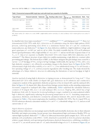
Table 2. Summarized compound MO single-layer and multi-stack layer properties for flexibility
T μ
Type of layer Channel materials Substrate max Bending radius (mm) FE 2 -1 -1 Gate dielectric Refs. Year
(°C) (cm ·V ·s )
Compound single layer IZO/SWNT - 350 2 63.4 SiN [128] 2012
x
InO/EC - 275 1.5 40 Electrolyte [129] 2023
IGZO:PI SiN /SiO 300 10 - HfO [130] 2022
x 2 x
IGZO:PETE - 380 3 3.5 SiN /SiO 2 [131] 2018
x
Multi-stack InO/indicone AlO 200 2 2.05 AlO [132] 2021
x x
layer
MO: Metal oxide; IZO: indium zinc oxide; SWNT: single-walled carbon nanotube; EC: ethyl cellulose; IGZO: indium gallium zinc oxide; PI:
polyimide.
be classified into three types: monolayer [72,113,114,134-137] , multilayer [82,98,138-140] , and doping process [141-146] . Rim et al.
demonstrated IGZO TFTs with Al O dielectrics on PI substrates using the direct light pattern (DLP)
3
2
process, achieving patterning sizes down to a minimum feature size of 3 μm for conductors,
semiconductors, and dielectrics . In Figure 5A, these dielectrics exhibited a high breakdown voltage and
[72]
-1
good capacitance of ~4.9 MV·cm and 46.3 nF at 1 kHz. The study is notable that the TFTs on PI substrates
5
showed good performance with a high mobility of ~84.4 cm ·V ·s and an on/off ratio of greater than 10 at
-1 -1
2
V 1.0 V. Hsu et al. reported on flexible TiO /IGZO TFTs with bilayer HfO /TiO dielectrics on PC
2
2
DS
x
substrates . The bilayer structure of gate dielectrics enables maintaining a high dielectric constant while
[82]
preventing gate leakage. The bottom layer of HfO in the bilayer mitigates the gate leakage issue caused by a
2
narrow ~3.3 eV bandgap of TiO , owing to its high bandgap. Additionally, the top layer of TiO , with a very
2
2
high dielectric constant (> 40), efficiently accumulates charges in the channel layer. In Figure 5B, the TFTs
-1 -1
2
demonstrated a high field-effect mobility of 61 cm ·V ·s , a low subthreshold swing of 125 mV/decade, a
low operating voltage of 1.5 V, and less property degradation after bending test. The study showed the
advantages of a bilayer dielectric structure in addressing the limitations of narrow bandgap in high-k
materials.
Another method of using high-k dielectrics is doping process, as demonstrated by Yang et al. . They
[141]
fabricated IZO TFTs with soluble Zr-doped AlO gate dielectrics on PI substrates and conducted a
x
comparative analysis of the quantitative dielectric properties of the Zr-doped AlO and the undoped AlO
x
x
films. In Figure 5C, Zr-doped AlO films showed lower leakage current density as the annealing temperature
x
decreased, compared to undoped AlO films. Additionally, Table 3 exhibited the calculated dielectric
x
constant of Zr-doped AlO (8.4-11.8) and undoped AlO (5.6-6.2). Doping AlO , which has a high
x
x
x
breakdown field, with Zr, known for its strong bonding to oxygen, resulted in an unprecedented soluble
high-k dielectric, significantly reducing the processing temperature to 250 °C. Annealing temperature,
capacitance, thickness, and dielectric constant by calculation between AlO and Zr-doped AlO were
x
x
compared in Table 3. This report emphasizes the feasibility of flexible IZO TFTs. The Zr-doped TFTs on
2
-1 -1
ITO/PI substrates showed a saturation mobility of 51 cm ·V ·s , a threshold voltage of 1.2 V, and an on/off
current ratio of ~10 .
4
High-k dielectrics of polymer
High-k polymer dielectrics are increasingly used in flexible and stretchable electronics due to their inherent
flexibility and simple processing. Several groups have demonstrated high-performance flexible TFTs on
various high-k polymer dielectrics [147-149] . Zhu et al. fabricated electrolyte-gated synaptic In O TFTs on a PI
2
3
substrate with polyethylene oxide (PEO) + LiClO dissolved in acetonitrile to form the polymer electrolyte
4
solution as gate dielectric and reported good performance electrical characteristics, exhibiting a mobility of
7.80 cm ·V ·s , an on/off current ratio of ~10 , and a threshold voltage of 0.55 V. As shown in Figure 5D, an
2
-1 -1
6