
Page 187 - Read Online
P. 187
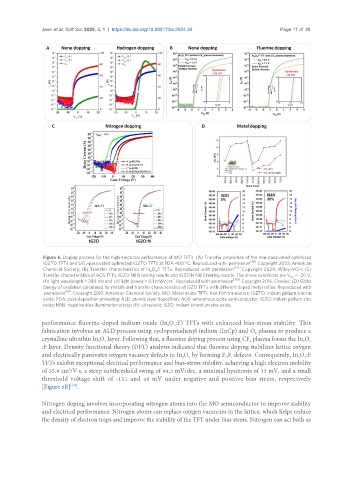
Jeon et al. Soft Sci. 2025, 5, 1  https://dx.doi.org/10.20517/ss.2024.35        Page 17 of 39


                Figure 6. Doping process for the high electrical performance of MO TFTs. (A) Transfer properties of the non-passivated optimized
                IGZTO TFTs and SiO -passivated optimized IGZTO TFTs at PDA 400 °C. Reproduced with  permission [59] . Copyright 2022, American
                              2
                Chemical Society; (B) Transfer characteristics of In O :F TFTs. Reproduced with  permission [173] . Copyright 2024, Wiley-VCH; (C)
                                                     3
                                                    2
                Transfer characteristics of AOS TFTs, IGZO NBIS testing results and IGZO:N NBIS testing results. The stress conditions are V  = -20 V,
                                                                                                   GS
                                                           2
                UV light wavelength = 380 nm and UV light power = 0.1 mW/cm . Reproduced with permission [159] . Copyright 2016, Elsevier; (D) Gibbs
                Energy of oxidation calculated for metals and transfer characteristics of ISZO TFTs with different doped metal ratios. Reproduced with
                permission [60] . Copyright 2013, American Chemical Society. MO: Metal oxide; TFTs: thin-film transistors; IGZTO: indium gallium zinc tin
                oxide; PDA: post-deposition annealing; ALD: atomic layer deposition; AOS: amorphous oxide semiconductor; IGZO: indium gallium zinc
                oxide; NBIS: negative bias illumination stress; UV: ultraviolet; ISZO: indium strontium zinc oxide.
               performance fluorine-doped indium oxide (In O :F) TFTs with enhanced bias-stress stability. This
                                                            3
                                                         2
               fabrication involves an ALD process using cyclopentadienyl indium (InCp) and O  plasma to produce a
                                                                                       2
               crystalline ultrathin In O  layer. Following that, a fluorine doping process using CF  plasma forms the In O 3
                                  2
                                    3
                                                                                                       2
                                                                                     4
               :F layer. Density functional theory (DFT) analysis indicated that fluorine doping stabilizes lattice oxygen
               and electrically passivates oxygen vacancy defects in In O  by forming F F defects. Consequently, In O :F
                                                                 3
                                                              2
                                                                             O i
                                                                                                        3
                                                                                                      2
               TFTs exhibit exceptional electrical performance and bias-stress stability, achieving a high electron mobility
               of 35.9 cm /V·s, a steep subthreshold swing of 94.3 mV/dec, a minimal hysteresis of 33 mV, and a small
                        2
               threshold voltage shift of -111 and 49 mV under negative and positive bias stress, respectively
               [Figure 6B] .
                         [173]
               Nitrogen doping involves incorporating nitrogen atoms into the MO semiconductor to improve stability
               and electrical performance. Nitrogen atoms can replace oxygen vacancies in the lattice, which helps reduce
               the density of electron traps and improve the stability of the TFT under bias stress. Nitrogen can act both as