
Page 185 - Read Online
P. 185
Jeon et al. Soft Sci. 2025, 5, 1 https://dx.doi.org/10.20517/ss.2024.35 Page 15 of 39
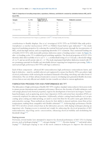
Table 3. Comparison of annealing temperature, capacitance, thickness, and dielectric constant by calculation between AlO and Zr-
x
doped AlO x
Capacitance at
Sample T (°C) 1 MHz (nF·cm ) Thickness Dielectric constant
-2
a
AlO 250 71 70 5.6
x
300 84 64 6.1
350 91 61 6.2
Zr-doped AlO x 250 70 106 8.4
300 90 100 10.2
350 110 95 11.8
[141]
This table is cited with permission from Yang et al., published in 2013 , The Royal Society of Chemistry.
contributions to flexible displays. Hur et al. investigated IGTO TFTs on PI/PMDS film with poly(4-
[149]
vinylphenol-co-methyl methacrylate) (PVP-co-PMMA)-based hybrid gate dielectrics . The study
improved insulating properties by reducing the residual hydroxyl groups through the incorporation of
HfO , which has high ionicity, and accompanying ultraviolet (UV) treatment. They conducted bending test
x
of flexible IGTO TFTs with stretchable polymer dielectrics under a bending radius (1 mm). In Figure 5E,
after 100 bending cycles, TFTs exhibited good switching capability. The electrical properties of IGTO TFTs
showed a field-effect mobility of 25.9 cm ·V ·s , a subthreshold swing of 0.4 V/decade, a threshold voltage
2
-1 -1
7
of -0.2 V, and an on/off current ratio of > 10 . The study emphasized that hybrid dielectrics treated with UV
are promising materials for flexible and stretchable devices requiring low-temperature processing. Table 4
summarized high-performance MO TFTs with high-k dielectrics.
Each of these components - advanced MO semiconductors, high-performance semiconductor layers, and
high-k dielectrics - must be carefully selected and engineered to ensure that flexible TFTs can achieve high
electrical performance while enduring the mechanical demands of bending, stretching, and other forms of
deformation. The use of these advanced materials is crucial in developing next-generation flexible electronic
devices that are not only efficient and reliable but also versatile and robust in various applications.
FABRICATION PROCESS FOR HIGH-PERFORMANCE MO TFT
The fabrication of high-performance flexible MO TFTs employs standard semiconductor fabrication tools
to ensure precise dimensions and consistent performance. However, the diversity of flexible substrates, each
with unique physical and chemical properties, requires the development of innovative techniques. Vacuum-
based techniques, such as sputtering, atomic layer deposition (ALD), and pulsed laser deposition (PLD), are
commonly employed for substrate deposition. Additionally, solution coating-based methods, such as spin
coating, spray coating and inkjet printing, are used to create thin films for the active layers, gate dielectrics,
and protective coatings. These methods are chosen for their ability to deposit uniform, dense films at low
temperatures, making them compatible with flexible substrates [8,15,95] . Achieving high-performance flexible
MO TFTs involves several critical steps in the fabrication process, with doping techniques playing an
important role. Doping process is essential and simple for enhancing the electrical properties of MO
semiconductors, improving carrier concentration, enhancing electrical stability and modulating the
threshold voltage [55,95] .
Doping process
Previously, several studies have attempted to improve the electrical performance of MO TFTs by doping
process, such as hydrogen doping [59,151-157] , nitrogen doping [110,113,157-161] , fluorine doping [162-168] and metal cation
doping [55-57,60] . Hydrogen doping is one of the most common techniques to improve the electrical