
Page 181 - Read Online
P. 181
Jeon et al. Soft Sci. 2025, 5, 1 https://dx.doi.org/10.20517/ss.2024.35 Page 11 of 39
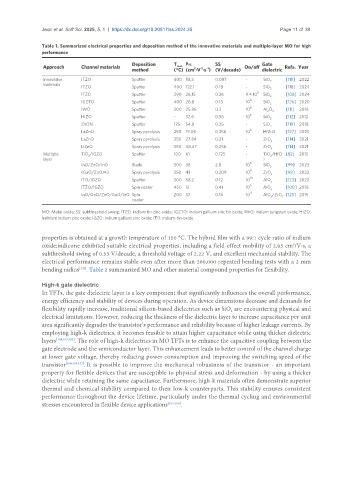
Table 1. Summarized electrical properties and deposition method of the innovative materials and multiple-layer MO for high
performance
Deposition T μ FE SS Gate
max
Approach Channel materials method (°C) (cm ·V ·s ) (V/decade) On/off dielectric Refs. Year
2
-1
-1
Innovative ITZO Sputter 400 58.3 0.087 - SiO [115] 2022
2
materials
ITZO Sputter 400 122.1 0.18 - SiO 2 [118] 2024
8
ITZO Sputter 290 26.15 0.26 9 × 10 SiO [108] 2024
2
IGZTO Sputter 400 26.8 0.15 10 8 SiO 2 [126] 2020
6
IWO Sputter 300 25.86 0.3 10 Al O [111] 2018
2 3
6
HIZO Sputter - 32.6 0.55 10 SiO 2 [112] 2012
ZnON Sputter 175 54.8 0.25 - SiO [119] 2018
2
8
LaZnO Spray pyrolysis 250 19.06 0.256 10 HfZrO [127] 2023
LaZnO Spray pyrolysis 350 27.84 0.21 - ZrO x [114] 2021
LiZnO Spray pyrolysis 350 48.47 0.256 - ZrO [114] 2021
x
Multiple TiO /IGZO Sputter 100 61 0.125 - TIO /HfO [82] 2015
2
2
layer 2
InO/ZnO/InO Blade 300 38 2.8 10 6 SiO 2 [99] 2023
8
(GaO/ZnO)×3 Spray pyrolysis 350 41 0.209 10 ZrO [98] 2022
x
10
ITO/IGZO Sputter 300 58.2 0.12 10 AlO x [123] 2023
ITZO/IGZO Spin coater 450 51 0.41 10 8 AlO x [100] 2018
4
InO/GaO/ZnO/GaO/InO Spin 200 37 0.16 10 AlO /ZrO [125] 2015
x 2
coater
MO: Metal oxide; SS: subthreshold swing; ITZO: indium tin zinc oxide; IGZTO: indium gallium zinc tin oxide; IWO: indium tungsten oxide; HIZO:
hafnium indium zinc oxide; IGZO: indium gallium zinc oxide; ITO: indium-tin-oxide.
properties is obtained at a growth temperature of 150 °C. The hybrid film with a 99:1 cycle ratio of indium
oxide:indicone exhibited suitable electrical properties, including a field-effect mobility of 2.05 cm /V·s, a
2
subthreshold swing of 0.53 V/decade, a threshold voltage of 2.22 V, and excellent mechanical stability. The
electrical performance remains stable even after more than 200,000 repeated bending tests with a 2 mm
bending radius . Table 2 summarized MO and other material compound properties for flexibility.
[132]
High-k gate dielectric
In TFTs, the gate dielectric layer is a key component that significantly influences the overall performance,
energy efficiency and stability of devices during operation. As device dimensions decrease and demands for
flexibility rapidly increase, traditional silicon-based dielectrics such as SiO are encountering physical and
2
electrical limitations. However, reducing the thickness of the dielectric layer to increase capacitance per unit
area significantly degrades the transistor’s performance and reliability because of higher leakage currents. By
employing high-k dielectrics, it becomes feasible to attain higher capacitance while using thicker dielectric
layers [104,105,133] . The role of high-k dielectrics in MO TFTs is to enhance the capacitive coupling between the
gate electrode and the semiconductor layer. This enhancement leads to better control of the channel charge
at lower gate voltage, thereby reducing power consumption and improving the switching speed of the
transistor [104,105,133] . It is possible to improve the mechanical robustness of the transistor - an important
property for flexible devices that are susceptible to physical stress and deformation - by using a thicker
dielectric while retaining the same capacitance. Furthermore, high-k materials often demonstrate superior
thermal and chemical stability compared to their low-k counterparts. This stability ensures consistent
performance throughout the device lifetime, particularly under the thermal cycling and environmental
stresses encountered in flexible device applications [103-105] .