
Page 194 - Read Online
P. 194
Page 24 of 39 Jeon et al. Soft Sci. 2025, 5, 1 https://dx.doi.org/10.20517/ss.2024.35
Junctionless structure
The flexible TFTs can experience stress concentration at the S/D and channel junction, potentially causing
deformation and delamination between the channel and the S/D electrodes which increase in contact
resistance under mechanical stress [63-66,194-198] . The increase in contact resistance degrades the device.
However, flexible MO TFTs employing junctionless structure have no S/D electrode and channel junction.
Therefore, mechanical stress is not concentrated at the S/D electrode and channel junction under
mechanical. It is also less affected by the change of contact resistance caused by mechanical stress. In 2021,
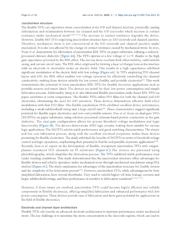
Yuan et al. demonstrate the fabrication of junctionless EDL TFTs on paper substrates, utilizing a solution-
processed chitosan dielectric [Figure 8A]. The TFTs operate at a low voltage of 1.0 V, thanks to the high
gate capacitance provided by the EDL effect. The devices show excellent field-effect mobility, subthreshold
swing, and current on/off ratio. The EDL effect originated by forming a layer of charged ions at the interface
with an electrode in electrolyte under an electric field. This results in a high capacitance exhibited
significant modulation of the electric field with low voltage [Figure 8A]. In TFTs employing ITO channel
layers and S/D, the EDL effect enables low-voltage operation by effectively controlling the channel
[66]
conductivity, making these devices suitable for low-power, flexible, and portable electronics . This work
demonstrates the potential of these junctionless EDL TFTs for flexible electronic applications such as
portable sensors and smart labels. The devices are noted for their low power consumption and simple
fabrication process. Additionally, Jiang et al. also fabricated flexible junctionless oxide-based EDL TFTs on
paper substrates at room temperature. The flexible TFTs utilize ITO films for both the channel and S/D
electrodes, eliminating the need for S/D junctions. These devices demonstrate effective field-effect
modulation with thin ITO films. The flexible junctionless TFTs exhibited excellent device performance,
[64]
including a small subthreshold swing and a large on/off ratio . These characteristics suggest significant
potential for flexible paper electronics and low-cost portable sensors. Dou et al. focus on dual-gate TFTs
(DGTFTs) on paper substrates, using solution-processed chitosan-based proton conductors as the gate
dielectric. The dual-gate configuration allows for precise threshold voltage modulation and logic
functionality [Figure 8B]. The devices demonstrate AND logic circuits, making them suitable for various
logic applications. The DGTFTs exhibit stable performance and good switching characteristics. The simple
and low-cost fabrication process, along with the excellent electrical properties, makes these devices
promising for flexible electronics. The study exhibited the benefits of DGTFTs in terms of threshold voltage
control and logic operations, emphasizing their potential in flexible and portable electronic applications .
[194]
Recently, Jeon et al. report on the development of flexible, transparent junctionless TFTs with oxygen-
plasma treatment ITO channels on PI substrates [Figure 8C]. The devices are patterned using
photolithography, which simplifies the fabrication process. The TFTs exhibited stable performance even
under bending conditions. This study demonstrated that the junctionless structure offers advantages for
flexible devices and reliable operation under mechanical stress through mechanical simulations using FEA
method [Figure 8C]. The study emphasizes the advantages of the junctionless structure for flexible devices
[198]
and the simplicity of the fabrication process . However, junctionless TFTs, while advantageous for their
simplified fabrication, have several drawbacks. They tend to exhibit higher off-state leakage currents and
larger subthreshold swings, and their performance is sensitive to fabrication variations [63-66,194-197] .
However, if these issues are resolved, junctionless TFTs could become highly efficient and reliable
components in flexible electronics, offering simplified fabrication and enhanced performance with low
power consumption. These devices provide ease of fabrication and show great potential for applications in
the field of flexible electronics.
Electrode and channel layer architecture
Flexible TFTs rely heavily on advanced electrode architectures to maintain performance under mechanical
stress. The key challenge is to minimize the stress concentration at the electrode regions, which can lead to