
Page 82 - Read Online
P. 82
Page 8 of 27 Kim et al. Soft Sci 2024;4:24 https://dx.doi.org/10.20517/ss.2024.09
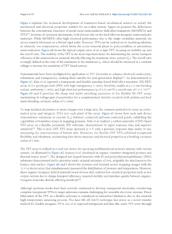
Figure 4 explains the technical development of transistor-based mechanical sensors to satisfy the
mechanical and electrical properties suitable for an e-skin system. Figure 4A presents the differences
between the conventional structures of metal-oxide-semiconductor field effect transistors (MOSFETs) and
[44]
TFTs . In terms of operation mechanism, both devices rely on the field effect in inorganic semiconductor
materials. While MOSFETs offer high electrical performance due to the single crystalline material, the
device must be fabricated on a limited rigid wafer. However, TFTs can be realized on an insulating substrate
at relatively low temperatures, which limits the active material phase to polycrystalline or amorphous
semiconductors. Figure 4B shows the typical output curve of an n-type TFT, focusing on mobility (μ) and
the on/off ratio. The mobility of the TFT is the most important factor for determining the carrier transport
efficiency of the semiconductor material, directly affecting the maximum drain current (I ). The on/off ratio
D
is simply defined as the ratio of the maximum to the minimum I , which should be enhanced at a constant
D
voltage to increase the sensitivity of TFT-based sensors.
Nanomaterials have been spotlighted for application to TFT electrodes to enhance electrical conductivity,
robustness, and transparency, making them suitable for next-generation displays . As demonstrated in
[45]
Figure 4C, Kim et al. reported a transparent and flexible nanoline-based field effect transistor (NL-FET)
array of 254 pixels-per-inch (PPI) with high transparency (~90%), flexibility (stable at a 2.5 mm bending
6 [46]
2
radius), uniformity (~90%), and high electrical performances (μ of 0.52 cm /V·s, on/off ratio of 7.0 × 10 ) .
Figure 4D and E provides the sharp and stable switching operation of the flexible NL-FET array,
maintaining its voltage gain characteristics for a complementary inverter circuit in both pristine and bent
states (bending curvature radius of 2.5 mm).
To map mechanical pressure or stress changes over a large area, the common method is to create an active-
matrix array and integrate TFTs into each pixel of the array. Figure 4F shows how each unit device
demonstrates variations in current (I ) between contacted and non-contacted pixels, exhibiting the
ON
capabilities of transistor arrays in mapping pressure. Nela et al. realized a carbon nanotube (CNT)-based
TFT array on a flexible polyimide (PI) substrate, characterized by rapid response time and superior
[47]
sensitivity . This 4-inch CNT TFT array operated at 3 V with a pressure response time under 30 ms,
surpassing the responsiveness of human skin. Moreover, the flexible CNT TFTs exhibited exceptional
flexibility and robustness, maintaining their device structure and electrical properties at a bending curvature
radius of 5 mm.
The TFT array is utilized as a read-out device for operating multifunctional network systems with various
sensors. As illustrated in Figure 4G, Someya et al. developed an organic transistor-integrated pressure and
thermal sensor array . The designed net-shaped structure with PI and poly(ethylenenaphthalate) (PEN)
[48]
substrates demonstrated stable operation under uniaxial extension of 25%, adaptable for attachment to the
human skin surface. Figure 4H and I shows the pressure and thermal sensor mapping images with the
12 × 12 device array that simultaneously measured the distribution of pressure and temperature. However,
these organic-inorganic hybrid material-based devices still confront low electrical properties such as low
output current due to charge transport efficiency, material stability and interface quality between organic-
inorganic materials, directly affecting sensitivity .
[49]
Although previous works have been actively conducted to develop transparent electrodes, transferring
complete transparent TFTs to target substrates remains challenging for wearable electronic systems. Direct
fabrication of the TFT on a flexible substrate is considered an unresolved limitation due to the essential
high-temperature annealing process. The laser lift-off (LLO) technique has arisen as a novel transfer
method for flexible inorganic TFTs. Lee et al. reported transparent and skin-like oxide TFT array through