
Page 79 - Read Online
P. 79
Kim et al. Soft Sci 2024;4:24 https://dx.doi.org/10.20517/ss.2024.09 Page 5 of 27
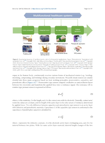
Figure 2. Developing sequence of multifunctional e-skins for biomedical applications. Figure “Photodetector” Reproduced with
permission from ref [23] . Copyright 2022, John Wiley and Sons; Figure “Flexible µLED” Reproduced with permission from ref [24] . Copyright
2022, American Chemical Society; Figure “Sensing device array” Reproduced with permission from ref [25] . Copyright 2019, Springer
Nature; Figure “Multi-functional sensing device” Reproduced with permission from ref [26] . Copyright 2007, Elsevier; Figure “Skin-
adhesive device” Reproduced with permission from ref [27] . Copyright 2016, Elsevier. Figure “Therapeutic application” Reproduced with
permission from ref [28] . Copyright 2020, Springer Nature; Figure “PPG sensor” Reproduced with permission from ref [29] . Copyright 2022,
AAAS. µLED: Micro-scale light-emitting diode; PPG: photoplethysmography.
organ in the human body, continuously receives various forms of mechanical strains (e.g., bending,
stretching, compressing, and twisting) during everyday movements. Wearable strain sensors are usually
divided into three main categories based on their working principles: piezoresistive, capacitive, and
piezoelectric effects [Figure 3A] . Piezoresistive type sensors comprise conductive or semiconductor layers
[34]
between two electrodes and transform the applied force into a resistance signal. The resistance (R) in
resistive type pressure sensor is expressed as follows:
where ρ is the resistivity, L is the length, and A is the contact area with the electrode. Generally, contact area/
resistivity values are constant, and the length of the active layer is the only variant of resistance determined
by applied force. The only difference between capacitive and piezoelectric type sensors is an active layer
with dielectric and piezoelectric materials. Capacitance C of the capacitive type sensors is conformed to the
capacitance of parallel plate capacitors calculated by:
where ε represents the dielectric constant, A is the electrode-active layer overlapping area, and d is the
interval between two plates. With the same active layer material, interval length changes of the two