
Page 83 - Read Online
P. 83
Kim et al. Soft Sci 2024;4:24 https://dx.doi.org/10.20517/ss.2024.09 Page 9 of 27
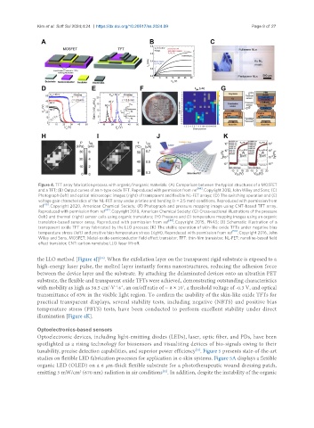
Figure 4. TFT array fabrication process with organic/inorganic materials. (A) Comparison between the typical structures of a MOSFET
[44]
and a TFT; (B) Output curves of an n-type oxide TFT. Reproduced with permission from ref . Copyright 2012, John Wiley and Sons; (C)
Photograph (left) and optical microscopic images (right) of transparent and flexible NL-FET arrays; (D) The switching operation and (E)
voltage gain characteristics of the NL-FET array under pristine and bending (r = 2.5 mm) conditions. Reproduced with permission from
ref [46] . Copyright 2020, American Chemical Society; (F) Photograph and pressure mapping image using CNT-based TFT array.
Reproduced with permission from ref [47] . Copyright 2018, American Chemical Society; (G) Cross-sectional illustrations of the pressure
(left) and thermal (right) sensor cells using organic transistors; (H) Pressure and (I) temperature mapping images using an organic
transistor-based sensor array. Reproduced with permission from ref [48] . Copyright 2015, PNAS; (J) Schematic illustration of a
transparent oxide TFT array fabricated by the LLO process; (K) The stable operation of skin-like oxide TFTs under negative bias
temperature stress (left) and positive bias temperature stress (right). Reproduced with permission from ref [50] . Copyright 2016, John
Wiley and Sons. MOSFET: Metal-oxide-semiconductor field effect transistor; TFT: thin-film transistor; NL-FET: nanoline-based field
effect transistor; CNT: carbon nanotube; LLO: laser lift-off.
the LLO method [Figure 4J] . When the exfoliation layer on the transparent rigid substrate is exposed to a
[50]
high-energy laser pulse, the melted layer instantly forms nanostructures, reducing the adhesion force
between the device layer and the substrate. By attaching the delaminated devices onto an ultrathin PET
substrate, the flexible and transparent oxide TFTs were achieved, demonstrating outstanding characteristics
with mobility as high as 38.5 cm ·V ·s , an on/off ratio of ~ 8 × 10 , a threshold voltage of -0.3 V, and optical
-1 -1
7
2
transmittance of 83% in the visible light region. To confirm the usability of the skin-like oxide TFTs for
practical transparent displays, several stability tests, including negative (NBTS) and positive bias
temperature stress (PBTS) tests, have been conducted to perform excellent stability under direct
illumination [Figure 4K].
Optoelectronics-based sensors
Optoelectronic devices, including light-emitting diodes (LEDs), laser, optic fiber, and PDs, have been
spotlighted as a rising technology for biosensors and visualizing devices of bio-signals owing to their
[51]
tunability, precise detection capabilities, and superior power efficiency . Figure 5 presents state-of-the-art
studies on flexible LED fabrication processes for application in e-skin systems. Figure 5A displays a flexible
organic LED (OLED) on a 6 μm-thick flexible substrate for a phototherapeutic wound dressing patch,
emitting 5 mW/cm (670 nm) radiation in air conditions . In addition, despite the instability of the organic
2
[52]