
Page 18 - Read Online
P. 18
Jan et al. Soft Sci 2024;4:10 https://dx.doi.org/10.20517/ss.2023.54 Page 7 of 12
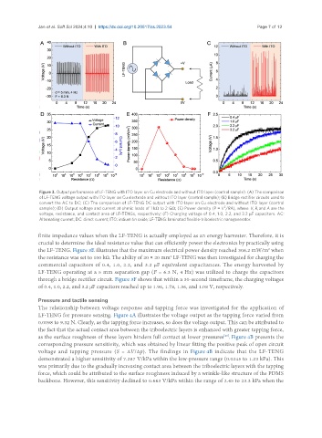
Figure 3. Output performance of LF-TENG with ITO layer on Cu electrode and without ITO layer (control sample). (A) The comparison
of LF-TENG voltage output with ITO layer on Cu electrode and without ITO layer (control sample); (B) Bridge rectifier circuits used to
convert the AC to DC; (C) The comparison of LF-TENG DC output with ITO layer on Cu electrode and without ITO layer (control
2
sample); (D) Output voltage and current at ohmic loads of 1 kΩ to 2 GΩ; (E) Power density (P = V /RA), where V, R, and A are the
voltage, resistance, and contact area of LF-TENGs, respectively; (F) Charging voltage of 0.4, 1.0, 2.2, and 3.2 μF capacitors. AC:
Alternating current; DC: direct current; ITO: indium tin oxide; LF-TENG: laminated flexible-triboelectric nanogenerator.
finite impedance values when the LF-TENG is actually employed as an energy harvester. Therefore, it is
crucial to determine the ideal resistance value that can efficiently power the electronics by practically using
the LF-TENG. Figure 3E illustrates that the maximum electrical power density reached 306.2 mW/m when
2
the resistance was set to 100 kΩ. The ability of 20 × 20 mm LF-TENG was then investigated for charging the
2
commercial capacitors of 0.4, 1.0, 2.2, and 3.2 μF equivalent capacitances. The energy harvested by
LF-TENG operating at a 5 mm separation gap (F = 6.3 N, 4 Hz) was utilized to charge the capacitors
through a bridge rectifier circuit. Figure 3F shows that within a 30-second timeframe, the charging voltages
of 0.4, 1.0, 2.2, and 3.2 μF capacitors reached up to 1.96, 1.78, 1.36, and 1.08 V, respectively.
Pressure and tactile sensing
The relationship between voltage response and tapping force was investigated for the application of
LF-TENG for pressure sensing. Figure 4A illustrates the voltage output as the tapping force varied from
0.0098 to 9.32 N. Clearly, as the tapping force increases, so does the voltage output. This can be attributed to
the fact that the actual contact area between the triboelectric layers is enhanced with greater tapping force,
[40]
as the surface roughness of these layers hinders full contact at lower pressures . Figure 4B presents the
corresponding pressure sensitivity, which was obtained by linear fitting the positive peak of open circuit
voltage and tapping pressure (S = ΔV/Δp). The findings in Figure 4B indicate that the LF-TENG
demonstrated a higher sensitivity of 7.287 V/kPa within the low-pressure range (0.0245 to 1.23 kPa). This
was primarily due to the gradually increasing contact area between the triboelectric layers with the tapping
force, which could be attributed to the surface roughness induced by a wrinkle-like structure of the PDMS
backbone. However, this sensitivity declined to 0.663 V/kPa within the range of 2.45 to 23.3 kPa when the