
Page 15 - Read Online
P. 15
Page 4 of 12 Jan et al. Soft Sci 2024;4:10 https://dx.doi.org/10.20517/ss.2023.54
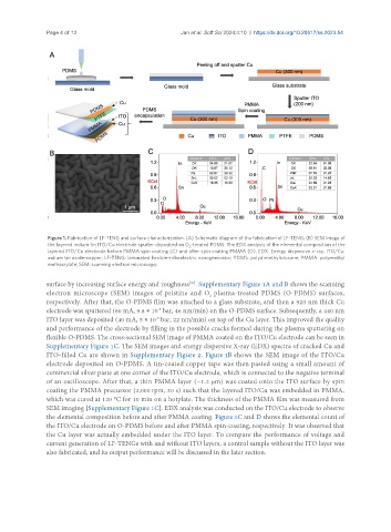
Figure 1. Fabrication of LF-TENG and surface characterization. (A) Schematic diagram of the fabrication of LF-TENG; (B) SEM image of
the layered indium tin ITO/Cu electrode sputter deposited on O -treated PDMS. The EDX analysis of the elemental composition of the
2
layered ITO/Cu electrode before PMMA spin coating (C) and after spin coating PMMA (D). EDX: Energy dispersive x-ray; ITO/Cu:
indium tin oxide-copper; LF-TENG: laminated flexible-triboelectric nanogenerator; PDMS: polydimethylsiloxane; PMMA: polymethyl
methacrylate; SEM: scanning electron microscopy.
surface by increasing surface energy and roughness . Supplementary Figure 1A and B shows the scanning
[36]
electron microscope (SEM) images of pristine and O plasma-treated PDMS (O-PDMS) surfaces,
2
respectively. After that, the O-PDMS film was attached to a glass substrate, and then a 920 nm thick Cu
electrode was sputtered (60 mA, 9.8 × 10 bar, 46 nm/min) on the O-PDMS surface. Subsequently, a 440 nm
-6
ITO layer was deposited (40 mA, 5 × 10 bar, 22 nm/min) on top of the Cu layer. This improved the quality
-6
and performance of the electrode by filling in the possible cracks formed during the plasma sputtering on
flexible O-PDMS. The cross-sectional SEM image of PMMA coated on the ITO/Cu electrode can be seen in
Supplementary Figure 1C. The SEM images and energy dispersive X-ray (EDX) spectra of cracked Cu and
ITO-filled Cu are shown in Supplementary Figure 2. Figure 1B shows the SEM image of the ITO/Cu
electrode deposited on O-PDMS. A tin-coated copper tape was then pasted using a small amount of
commercial silver paste at one corner of the ITO/Cu electrode, which is connected to the negative terminal
of an oscilloscope. After that, a thin PMMA layer (~1.2 μm) was coated onto the ITO surface by spin
coating the PMMA precursor (2,000 rpm, 30 s) such that the layered ITO/Cu was embedded in PMMA,
which was cured at 120 °C for 10 min on a hotplate. The thickness of the PMMA film was measured from
SEM imaging [Supplementary Figure 1C]. EDX analysis was conducted on the ITO/Cu electrode to observe
the elemental composition before and after PMMA coating. Figure 1C and D shows the elemental count of
the ITO/Cu electrode on O-PDMS before and after PMMA spin-coating, respectively. It was observed that
the Cu layer was actually embedded under the ITO layer. To compare the performance of voltage and
current generation of LF-TENGs with and without ITO layers, a control sample without the ITO layer was
also fabricated, and its output performance will be discussed in the later section.