Page 9 - Read Online
P. 9

Page 4 of 10       Ouyang et al. Microstructures 2023;3:2023027  https://dx.doi.org/10.20517/microstructures.2023.22

               Table 1. Magnetron sputtering parameters of BaTiO  film heterostructures
                                                   3
                Structure type                  BaTiO /Pt/Ti                       BaTiO /LaNiO /Pt/Ti
                                                     3
                                                                                       3
                                                                                             3
                                                                                      -4
                                                    -4
                Base pressure                   2 × 10  Pa                         2 × 10  Pa
                Pt/Ti layer sputtering pressure   0.3 Pa                           0.3 Pa
                Pt/Ti layer thickness           ~150-200 nm
                Buffer layer sputtering temperature   N/A                          500 °C
                Buffer layer sputtering atmosphere  N/A                            Ar:O  (4:1)
                                                                                      2
                Buffer layer sputtering pressure   N/A                             0.3 Pa
                Buffer layer thickness          N/A                                ~100 nm
                BaTiO  sputtering temperature   500 °C                             500 °C
                   3
                BaTiO  sputtering atmosphere    Ar:O  (4:1)                        Ar:O  (4:1)
                   3                               2                                  2
                BaTiO  sputtering pressure      0.3 Pa                             1.2 Pa
                   3
                BaTiO  deposition rate          ~7 nm/min                          ~10 nm/min
                   3
                BaTiO  layer thickness (nm)     435 nm, 845 nm, 1,305 nm, 2,610 nm   510 nm
                   3
                Cooling atmosphere (pressure)   Pure O  (2.5 Pa)                   Pure O  (2.5 Pa)
                                                    2                                  2


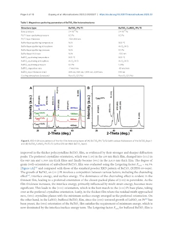
                Figure 1. XRD θ-2θ scan patterns of the thin film heterostructures of (A) BaTiO /Pt/Ti/Si (with various thicknesses of the BaTiO  layer)
                                                                    3
                                                                                                     3
                and (B) BaTiO /LaNiO /Pt/Ti/Si (with a 510 nm thick BaTiO  layer).
                                                        3
                         3
                               3
               improved in the thicker polycrystalline BaTiO  film, as evidenced by their stronger and sharper diffraction
                                                      3
               peaks. The preferred crystalline orientation, which was (110) in the 435 nm thick film, changed into (111) in
               the 845 nm and 1,305 nm thick films and finally became (001) in the 2,610 nm thick film. The degree of
               grain (00l)-orientation of unbuffered BaTiO  film was evaluated using the Lotgering factor F  = 64.7%
                                                      3
                                                                                                (00l)
               [Figure 1A]  and compared with those of the standard powder XRD pattern of BaTiO  (JCPDS 05-0626).
                         [16]
                                                                                          3
               The growth of BaTiO  on (111) Pt involves a competition between various factors, including the channeling
                                 3
               effect , interface energy, and surface energy. The dominance of the channeling effect is evident in the
                    [17]
               thinnest film, leading to a preferred orientation of the closest-packed plane of (110) in perovskite. As the
               film thickness increases, the interface energy, primarily influenced by misfit strain energy, becomes more
               significant. This leads to the (111) orientation, which is the best match to the (111) Pt base plane, taking
               over as the preferred crystalline orientation. Lastly, in the thickest film where the residual misfit approached
               zero, (001) crystalline planes with the minimum surface energy emerged as the preferred orientation. On
               the other hand, in the LaNiO -buffered BaTiO  film, since the (100)-textured growth of LaNiO  on Pt  has
                                                                                                     [18]
                                                                                               3
                                        3
                                                      3
               been preset, the (001) orientation of the BaTiO  film satisfies the requirement of minimum energy, which is
                                                       3
               now dominated by the interface/surface energy term. The Lotgering factor F  for buffered BaTiO  film is
                                                                                (00l)
                                                                                                   3
   4   5   6   7   8   9   10   11   12   13   14