
Page 10 - Read Online
P. 10
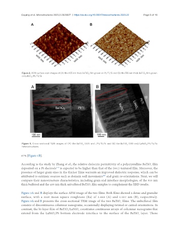
Ouyang et al. Microstructures 2023;3:2023027  https://dx.doi.org/10.20517/microstructures.2023.22  Page 5 of 10


                Figure 2. AFM surface scan images of (A) the 435 nm thick BaTiO  film grown on Pt/Ti/Si and (B) the 510 nm thick BaTiO  film grown
                                                            3                                    3
                on LaNiO /Pt/Ti/Si.
                      3


                Figure 3. Cross-sectional TEM images of (A) the BaTiO  (435 nm) /Pt/Ti/Si and (B) the BaTiO  (510 nm)/LaNiO /Pt/Ti/Si
                                                        3
                                                                                                  3
                                                                                     3
                heterostructures.
               87% [Figure 1B].

               According to the study by Zhang et al., the relative dielectric permittivity of a polycrystalline BaTiO  film
                                                                                                     3
                                      [19]
               deposited on a Pt electrode  is expected to be higher than that of the (001)-textured film. Moreover, the
               presence of larger grain sizes in the thicker films warrants an improved dielectric response, which can be
                                                                     [20]
               attributed to extrinsic sources such as domain wall movements  and grain re-orientations. Next, we will
               compare their nanostructure characteristics, including grain and interface morphologies, of the 510 nm
               thick buffered and the 435 nm thick unbuffered BaTiO  film samples to complement the XRD results.
                                                             3
               Figure 2A and B displays the surface AFM image of the two films. Both films showed a dense and granular
               surface,  with  a  root  mean  square  roughness  (Ra)  of  2.868  (A)  and  2.007  nm  (B),  respectively.
               Figure 3A and B presents the cross-sectional TEM image of the two BaTiO  films. The unbuffered film
                                                                                 3
               consists of discontinuous columnar nanograins, occasionally displaying twisted or canted orientations. In
               contrast, the bi-layer film of BaTiO /LaNiO  constitutes continuous arrays of columnar nanograins that
                                                     3
                                              3
               extend from the LaNiO /Pt bottom electrode interface to the surface of the BaTiO  layer. These
                                     3
                                                                                             3