
Page 11 - Read Online
P. 11
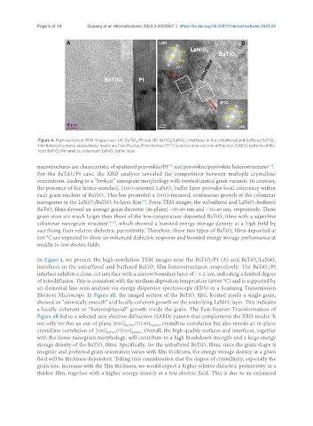
Page 6 of 10       Ouyang et al. Microstructures 2023;3:2023027  https://dx.doi.org/10.20517/microstructures.2023.22


                Figure 4. High-resolution TEM images near (A) BaTiO /Pt and (B) BaTiO /LaNiO  interfaces in the unbuffered and buffered BaTiO   3
                                                                  3
                                                                       3
                                                     3
                film heterostructures, respectively. Insets are Fast-Fourier-Transformed (FFT) selected area electron diffraction (SAED) patterns of the
                local BaTiO  film and its underneath LaNiO  buffer layer.
                       3
                                            3
                                                                 [17]
               nanostructures are characteristic of sputtered perovskite/Pt  and perovskite/perovskite heterostructures .
                                                                                                       [13]
               For the BaTiO /Pt case, the XRD analysis revealed the competition between multiple crystalline
                             3
               orientations, leading to a “broken” nanograin morphology with twisted/canted grain variants. In contrast,
               the presence of the lattice-matched, (100)-oriented LaNiO  buffer layer provides local coherency within
                                                                  3
               each grain nucleus of BaTiO . This has promoted a (001)-textured, continuous growth of the columnar
                                        3
                                                       [13]
               nanograins in the LaNiO /BaTiO  bi-layer film . From TEM images, the unbuffered and LaNiO -buffered
                                           3
                                                                                                 3
                                    3
               BaTiO  films showed an average grain diameter (in-plane) ~50-60 nm and ~30-40 nm, respectively. These
                     3
               grain sizes are much larger than those of the low-temperature deposited BaTiO  films with a superfine
                                                                                     3
               columnar nanograin structure [13-15] , which showed a boosted energy storage density at a high field by
               sacrificing their relative dielectric permittivity. Therefore, these two types of BaTiO  films deposited at
                                                                                         3
               500 °C are expected to show an enhanced dielectric response and boosted energy storage performance at
               middle-to-low electric fields.
               In Figure 4, we present the high-resolution TEM images near the BaTiO /Pt (A) and BaTiO /LaNiO 3
                                                                                 3
                                                                                                  3
               interfaces in the unbuffered and buffered BaTiO  film heterostructures, respectively. The BaTiO /Pt
                                                           3
                                                                                                       3
               interface exhibits a clean-cut interface with a narrow boundary layer of ~1-2 nm, indicating a limited degree
               of interdiffusion. This is consistent with the medium deposition temperature (@500 °C) and is supported by
               an elemental line scan analysis via energy dispersive spectroscopy (EDS) in a Scanning Transmission
               Electron Microscope. In Figure 4B, the imaged section of the BaTiO  film, located inside a single grain,
                                                                           3
               showed an “atomically smooth” and locally-coherent growth on the underlying LaNiO  layer. This indicates
                                                                                        3
               a locally coherent or “heteroepitaxial” growth inside the grain. The Fast-Fourier-Transformation of
               Figure 4B led to a selected area electron diffraction (SAED) pattern that complements the XRD results. It
               not only verifies an out-of-plane (001) BaTiO3 //(100) LaNiO3  crystalline correlation but also reveals an in-plane
               crystalline correlation of [100] BaTiO3 //(010) LaNiO3 . Overall, the high-quality surfaces and interfaces, together
               with the dense nanograin morphology, will contribute to a high breakdown strength and a large energy
               storage density of the BaTiO  films. Specifically, for the unbuffered BaTiO  films, since the grain shape is
                                        3
                                                                               3
               irregular and preferred grain orientation varies with film thickness, the energy storage density at a given
               field will be thickness-dependent. Taking into consideration that the degree of crystallinity, especially the
               grain size, increases with the film thickness, we would expect a higher relative dielectric permittivity in a
               thicker film, together with a higher energy density at a low electric field. This is due to an enhanced