Page 133 - Read Online
P. 133

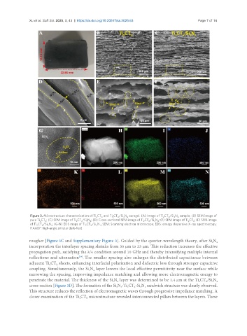
Xu et al. Soft Sci. 2025, 5, 43  https://dx.doi.org/10.20517/ss.2025.63          Page 7 of 16


                Figure 3. Microstructure characterization of Ti CT  and Ti CT /Si N  aerogel. (A) Image of Ti CT /Si N  sample; (B) SEM image of
                                               2  X    2  X  3  4               2  X  3  4
                pure Ti CT ; (C) SEM image of Ti CT /Si N ; (D) Cross-sectional SEM image of Ti CT /Si N ; (E) SEM image of Ti CT ; (F) SEM image
                    2  X              2  x  3  4                      2  X  3  4            2  X
                of Ti CT /Si N ; (G-N) EDS maps of Ti CT /Si N . SEM: Scanning electron microscope; EDS: energy dispersive X-ray spectroscopy;
                   2  X  3  4             2  X  3  4
                HAADF: high-angle annular dark-field.
               rougher [Figure 3C and Supplementary Figure 3]. Guided by the quarter-wavelength theory, after Si N
                                                                                                         4
                                                                                                       3
               incorporation the interlayer spacing shrinks from 30 µm to 23 µm. This reduction increases the effective
               propagation path, satisfying the λ/4 condition around 10 GHz and thereby intensifying multiple internal
               reflections and attenuation . The smaller spacing also enlarges the distributed capacitance between
                                       [58]
               adjacent Ti CT  sheets, enhancing interfacial polarization and dielectric loss through stronger capacitive
                            X
                         2
               coupling. Simultaneously, the Si N  layer lowers the local effective permittivity near the surface while
                                            3
                                              4
               narrowing the spacing, improving impedance matching and allowing more electromagnetic energy to
               penetrate the material. The thickness of the Si N  layer was determined to be 1.4 μm at the Ti CT /Si N
                                                          4
                                                                                                 2
                                                                                                         4
                                                                                                       3
                                                                                                    X
                                                       3
               cross-section [Figure 3D]. The formation of the Si N -Ti CT -Si N  sandwich structure was clearly observed.
                                                                     3
                                                                       4
                                                           4
                                                         3
                                                                  X
                                                              2
               This structure reduces the reflection of electromagnetic waves through progressive impedance matching. A
               closer examination of the Ti CT  microstructure revealed interconnected pillars between the layers. These
                                           X
                                       2
   128   129   130   131   132   133   134   135   136   137   138