
Page 28 - Read Online
P. 28
Page 10 of 43 Wang et al. Soft Sci 2024;4:41 https://dx.doi.org/10.20517/ss.2024.53
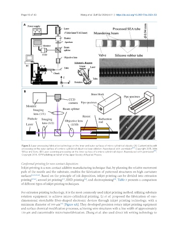
Figure 3. Laser processing fabrication technology on the inner and outer surfaces of micro-cylindrical objects. (A) Customizable path
processing on the outer surface of a micro-cylindrical object via laser ablation. Reproduced with permission [82] . Copyright 2011, John
Wiley and Sons; (B) Laser scanning processing on the inner surface of a micro-cylindrical object. Reproduced with permission [17] .
Copyright 2014, IOP Publishing on behalf of the Japan Society of Applied Physics.
Conformal printing for non-contact deposition
Inkjet printing is a non-contact additive manufacturing technique that, by planning the relative movement
path of the nozzle and the substrate, enables the fabrication of patterned structures on high-curvature
surfaces [12,83,85,86] . Based on the principle of ink deposition, inkjet printing can be divided into extrusion
[14]
[13]
printing [87,88] , aerosol jet printing , EHD printing , and electrospinning . Table 3 presents a comparison
[89]
of different types of inkjet printing techniques.
For extrusion printing technology, it is the most commonly used inkjet printing method, utilizing substrate
rotation equipment to achieve micro-cylindrical printing. Li et al. proposed the fabrication of one-
dimensional stretchable fiber-shaped electronic devices through inkjet printing technology, with a
[15]
minimum diameter of 500 μm [Figure 4A]. They developed precision rotary inkjet printing equipment
and surface chemical modification processes, achieving wire structures with a line width of approximately
130 μm and customizable micro/nanofabrication. Zhang et al. also used direct ink writing technology to