
Page 26 - Read Online
P. 26
Page 8 of 43 Wang et al. Soft Sci 2024;4:41 https://dx.doi.org/10.20517/ss.2024.53
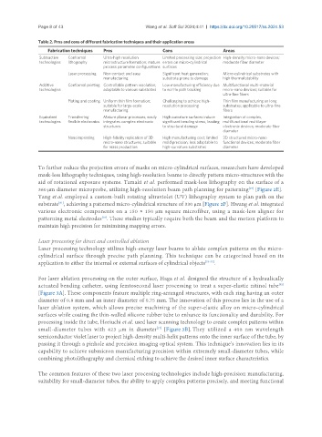
Table 2. Pros and cons of different fabrication techniques and their application areas
Fabrication techniques Pros Cons Areas
Subtractive Conformal Ultra-high resolution Limited processing size; projection High-density micro-nano devices;
technologies lithography microstructure formation; mature errors on micro-cylindrical moderate fiber diameter
process parameter configurations surfaces
Laser processing Non-contact and easy Significant heat generation; Micro-cylindrical substrates with
manufacturing substrate prone to damage high thermal stability
Additive Conformal printing Controllable pattern resolution; Low manufacturing efficiency due Multifunctional multi-material
technologies adaptable to various substrates to nozzle path tracking micro-nano devices; suitable for
ultra-fine fibers
Plating and coating Uniform thin film formation; Challenging to achieve high- Thin film manufacturing on long
suitable for large-scale resolution processing substrates; applicable to ultra-fine
manufacturing fibers
Equivalent Transferring Mature planar processes; easily High curvature surfaces induce Integration of complex,
technologies flexible electronics integrates complex electronic significant bending stress, leading multifunctional multilayer
structures to structural damage electronic devices; moderate fiber
diameter
Nanoimprinting High-fidelity replication of 3D High manufacturing cost; limited 3D structured micro-nano
micro-nano structures; suitable mold precision; less adaptable to functional devices; moderate fiber
for mass production high-curvature substrates diameter
To further reduce the projection errors of masks on micro-cylindrical surfaces, researchers have developed
mask-less lithography techniques, using high-resolution beams to directly pattern micro-structures with the
aid of rotational exposure systems. Tamaki et al. performed mask-less lithography on the surface of a
[19]
360 μm diameter microprobe, utilizing high-resolution beam path planning for patterning [Figure 2E].
Yang et al. employed a custom-built rotating ultraviolet (UV) lithography system to plan path on the
[81]
substrate , achieving a patterned micro-cylindrical structure of 330 μm [Figure 2F]. Hwang et al. integrated
various electronic components on a 150 × 150 μm square microfiber, using a mask-less aligner for
[18]
patterning metal electrodes . These studies typically require both the beam and the motion platform to
maintain high precision for minimizing mapping errors.
Laser processing for direct and controlled ablation
Laser processing technology utilizes high-energy laser beams to ablate complex patterns on the micro-
cylindrical surface through precise path planning. This technique can be categorized based on its
application to either the internal or external surfaces of cylindrical objects [75-77] .
For laser ablation processing on the outer surface, Haga et al. designed the structure of a hydraulically
[82]
actuated bending catheter, using femtosecond laser processing to treat a super-elastic nitinol tube
[Figure 3A]. These components feature multiple ring-arranged structures, with each ring having an outer
diameter of 0.8 mm and an inner diameter of 0.75 mm. The innovation of this process lies in the use of a
laser ablation system, which allows precise machining of the super-elastic alloy on micro-cylindrical
surfaces while coating the thin-walled silicone rubber tube to enhance its functionality and durability. For
processing inside the tube, Horiuchi et al. used laser scanning technology to create complex patterns within
small-diameter tubes with 423 μm in diameter [Figure 3B]. They utilized a 408 nm wavelength
[17]
semiconductor violet laser to project high-density multi-helix patterns onto the inner surface of the tube, by
passing it through a pinhole and precision imaging optical system. This technique’s innovation lies in its
capability to achieve submicron manufacturing precision within extremely small-diameter tubes, while
combining photolithography and chemical etching to achieve the desired inner surface characteristics.
The common features of these two laser processing technologies include high-precision manufacturing,
suitability for small-diameter tubes, the ability to apply complex patterns precisely, and meeting functional