
Page 71 - Read Online
P. 71
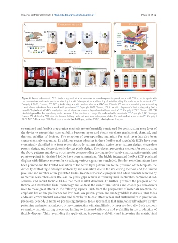
Wu et al. Soft Sci 2024;4:29  https://dx.doi.org/10.20517/ss.2024.21            Page 17 of 22


                Figure 11. Recent advances in ECD pixels integrated with various sensors based on point-to-point mode. (A) ECD pixels integrate with
                                                                                                        [28]
                the temperature and strain sensors detecting the skin’s temperature and bending of wrist bending. Reproduced with  permission  .
                                                                      +
                Copyright 2023, Elsevier; (B) ECD pixels integrate with various chemical (Na  and Vitamin C) sensors visualizing corresponding
                                                    [65]
                chemical concentrations. Reproduced with permission  . Copyright 2021, Elsevier; (C) Schematic diagram of a device integrating PANI-
                                                                                [120]
                based ECD pixels with PVDF-based piezo electrical pressure sensor. Reproduced with permission  . Copyright 2022, Elsevier; (D) ECD
                                                                                       [51]
                pixels triggered by the stretching state because of the resistance change. Reproduced with  permission  . Copyright 2021, Springer
                                                                                                 [27]
                Nature; (E) Multicolor ECD pixels indicate a battery meter with corresponding color states. Reproduced with permission  . Copyright
                2021, ACS Publications. ECD: Electrochromic display; PANI: polyaniline; PVDF: polyvinylidene fluoride.
               streamlined and feasible preparation methods are preferentially considered for constructing every layer of
               the device to ensure high compatibility between layers and obtain excellent mechanical, chemical, and
               thermal stability of devices. The selection of corresponding materials for each layer has also been
               comprehensively elaborated. In addition, recent advances in these flexible and stretchable ECDs have been
               systemically classified into four types: electrode pattern design, active layer pattern design, electrolyte
               pattern design, and electrochromic devices pixels design. The relevant processing methods for constructing
               the above patterns and device structure for corresponding driving modes (passive matrix, active matrix, and
               point-to-point) in pixelated ECDs have been summarized. The highly integrated flexible ECD pixelated
               displays with different sensors for visualizing various signals are concluded. Besides, some limitations have
               been pointed out: the limited resolution of the active layer pattern due to the precision of the template, the
               difficulty controlling electrolyte uniformity and resolution due to the UV curing method, and the limited
               pixel size and number of the pixelated ECDs. Despite remarkable progress and advancements achieved by
               numerous researchers over the last few years, gaps remain in realizing manufacturable, commercialized,
               scalable, and robust flexible ECDs that meet market demands. To further promote the progress of the
               flexible and stretchable ECD technology and address the current limitations and challenges, researchers
               need to make great efforts in the following aspects: First, from the perspective of materials selection, the
               emphasis lies on the preference for low-cost, low-power, green, and biodegradable materials. This focus
               addresses environmental concerns and contributes to cost-effectiveness and sustainability in production
               processes. Second, in terms of processing methods, facile approaches that simultaneously achieve display
               patterning and materials microstructure construction with simplified structures are desirable. Such methods
               streamline manufacturing processes, leading to increased efficiency and scalability in the production of
               flexible displays. Third, regarding the applications, improving scalability and increasing the matrix/pixel