
Page 144 - Read Online
P. 144
Lee et al. Soft Sci 2024;4:38 https://dx.doi.org/10.20517/ss.2024.36 Page 5 of 31
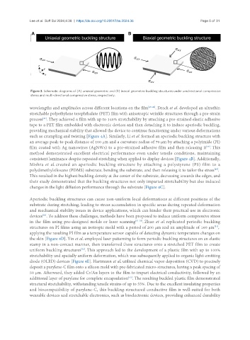
Figure 3. Schematic diagrams of (A) uniaxial geometric and (B) biaxial geometric buckling structures under unidirectional compressive
stress and multi-directional compressive stress, respectively.
wavelengths and amplitudes across different locations on the film [45-49] . Drack et al. developed an ultrathin
stretchable polyethylene terephthalate (PET) film with anisotropic wrinkle structures through a pre-strain
[45]
process . They achieved a film with up to 140% stretchability by attaching a pre-strained elastic adhesive
tape to a PET film embedded with electronic devices and then detaching it to induce aperiodic buckling,
providing mechanical stability that allowed the device to continue functioning under various deformations
such as crumpling and twisting [Figure 4A]. Similarly, Li et al. formed an aperiodic buckling structure with
an average peak-to-peak distance of 100 μm and a curvature radius of 70 μm by attaching a polyimide (PI)
[47]
film coated with Ag nanowires (AgNWs) to a pre-strained adhesive film and then releasing it . This
method demonstrated excellent electrical performance even under tensile conditions, maintaining
consistent luminance despite repeated stretching when applied to display devices [Figure 4B]. Additionally,
Mishra et al. created an aperiodic buckling structure by attaching a polystyrene (PS) film to a
[49]
polydimethylsiloxane (PDMS) substrate, bending the substrate, and then releasing it to tailor the stress .
This resulted in the highest buckling density at the center of the substrate, decreasing towards the edges, and
their study demonstrated that the buckling structures not only imparted stretchability but also induced
changes in the light diffusion performance through the substrate [Figure 4C].
Aperiodic buckling structures can cause non-uniform local deformations at different positions of the
substrate during stretching, leading to stress accumulation in specific areas during repeated deformation
and mechanical stability issues in device applications, which can hinder their practical use in electronic
devices . To address these challenges, methods have been proposed to induce uniform compressive stress
[50]
in the film using pre-designed molds or laser scanning [51-53] . Zhao et al. replicated periodic buckling
[51]
structures on PI films using an isotropic mold with a period of 200 μm and an amplitude of 160 μm ,
applying the resulting PI film as a temperature sensor capable of detecting dynamic temperature changes on
the skin [Figure 4D]. Yin et al. employed laser patterning to form periodic buckling structures on an elastic
stamp in a non-contact manner, then transferred these structures onto a stretched PET film to create
uniform buckling structures . This approach led to the development of a plastic film with up to 100%
[52]
stretchability and spatially uniform deformation, which was subsequently applied to organic light-emitting
diode (OLED) devices [Figure 4E]. Hartmann et al. utilized chemical vapor deposition (CVD) to precisely
deposit a parylene-C film onto a silicon mold with pre-fabricated micro-structures, having a peak spacing of
50 μm. Afterward, they added Cr/Au layers to the film to impart electrical conductivity, followed by an
[53]
additional layer of parylene for complete encapsulation . The resulting buckled plastic film demonstrated
structural stretchability, withstanding tensile strains of up to 55%. Due to the excellent insulating properties
and biocompatibility of parylene-C, this buckling-structured conductive film is well-suited for both
wearable devices and stretchable electronics, such as bioelectronic devices, providing enhanced durability