


Page 48 - Read Online
P. 48
Page 8 of 15                          Allen et al. J Mater Inf 2024;4:35  https://dx.doi.org/10.20517/jmi.2024.72


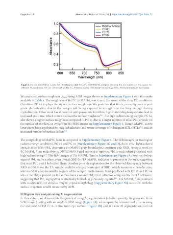
                Figure 1. UV-vis absorbance curves for TA reference and three PC ITO/MAPbI  samples showing the discrepancy of the curves for
                                                                      3
                different PC conditions. UV-vis: Ultraviolet-visible; PC: Photonic curing; ITO: Indium tin oxide; MAPbI : Methylammonium lead iodide.
                                                                                  3
               We measured surface roughness (σ ) using AFM images shown in Supplementary Figure 4 with the results
                                            RMS
               available in Table 1. The roughness of the PC 25 MAPbI  was 12 nm, the lowest of the three PC conditions.
                                                               3
               Condition PC 03 displays the highest surface roughness. We postulate that this is caused by poor crystal
               grain planarization due to the sample not being exposed to enough heat for long enough during
               crystallization. Other work has shown that with perovskite thin films, higher annealing temperatures lead to
               increased grain size, which in turn reduces the surface roughness . The high radiant energy sample, PC 04,
                                                                      [36]
               also shows a higher surface roughness compared to PC 25 due to a larger number of small PbI  crystals on
                                                                                                2
               the surface of the film, as evident in the SEM images in Supplementary Figure 5. Rough MAPbI  active
                                                                                                    3
                                                                                                 [37]
               layers have been attributed to reduced adhesion and worse coverage of subsequent ETLs/HTLs , and an
               increased number of surface defects .
                                             [38]
               The morphology of MAPbI  films is compared in Supplementary Figure 5. The SEM images for two higher
                                      3
               radiant energy conditions, PC 25 and PC 04 [Supplementary Figure 5C and D], show small light-colored
               crystals, most likely PbI , decorating the MAPbI  grain boundaries, consistent with XRD. Previous work on
                                                        3
                                   2
               PC MAPbI  films made from a DMF/DMSO-based recipe also reported PbI  crystals when processed with
                         3
                                                                                2
               high radiant energy . The SEM images of TA MAPbI  films in Supplementary Figure 5A show no obvious
                                [7]
                                                             3
               signs of PbI  on the surface, even though XRD for TA MAPbI  indicates its presence in the bulk, suggesting
                         2
                                                                   3
               that most PbI  could be located there. Another possible explanation for the observed discrepancy between
                           2
               XRD and SEM for the TA sample could be a larger beam spot of XRD, which measures a broader area,
               whereas SEM analyzes smaller regions of the sample. Furthermore, films produced with PC 25 and PC 04
               where the PbI  is present on the surface have a weaker PbI  (001) reflection compared to the TA reference,
                                                                 2
                           2
               suggesting that PbI  segregation is kinetically limited, as previously reported . The MAPbI  film produced
                                                                                [7]
                               2
                                                                                             3
               with condition PC 03 shows a rougher crystal morphology [Supplementary Figure 5B] consistent with the
               surface roughness results measured by AFM.
               SEM grain size analysis using AI segmentation
               In this section, we demonstrate the power of using AI segmentation to better quantify the grain size in an
               SEM image. Starting with an unedited SEM image [Figure 3A], we compare the conventional process using
               the standard ASTM E112-13 line intercept method [Figure 3B] and the new AI segmentation method

