
Page 153 - Read Online
P. 153
Page 8 of 35 Martin-Gonzalez et al. Energy Mater. 2025, 5, 500121 https://dx.doi.org/10.20517/energymater.2025.32
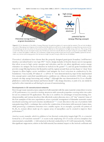
Figure 3. (A) An illustration of the effect of energy filtering at the grain boundaries of a nanocrystalline material. The vertical elevations
are a plot of the energy level diagram at the interfaces that the electrons will find, to visually explain the energy filtering process and the
potential energy barriers (in yellow) at the grain boundaries, which act as filtering barriers for high-energy electrons. The energy of the
current flow (blue arrows) increases locally near the barriers (electrons absorb phonons and gain energy to overpass them) which
locally increases the Seebeck coefficient. (B) A schematic of high-energy electrons passing through a grain boundary (potential barrier),
where only carriers with energy greater than the barrier height can pass through, while the rest are blocked.
Theoretical calculations have shown that the properly designed grain/grain-boundary (well/barrier)
interface can indeed lead to very high PFs . Such a design includes (i) heavily doped, narrow nanograins
[74]
that allow access to high carrier energies and velocities, and do not allow significant carrier energy
relaxation (to mitigate the local reduction in Seebeck in the grains [64,75] ); and (ii) grain-boundaries that
provide energy filtering barriers, but themselves and the regions around them are less doped or ‘clean’ from
dopants to allow higher carrier mobilities (and mitigate the local reduction in conductivity by the
-1
boundaries). Very recently, PF values of ~11 mW·m ·K were demonstrated in p-type Si that implemented
-2
this concept under controlled nanofabrication conditions on a Silicon-on-Insulator (SOI) wafer, a step
towards on-chip energy harvesting and cooling . Although this was demonstrated for Si as a flexible
[76]
platform to control the nano-feature and barrier details , this design direction, or parts of it, can widely be
[77]
applied to other materials as well during the process of nanostructuring.
Developments in 3D nanostructured networks
Even though many nanostructures outperform bulk materials with the same material composition in terms
of TE performance, it is crucial to develop structures with nanoscale properties covering wider size scales
for use in commercial TE applications. The idea is to combine the advantages of nanostructuring, low-
dimensionality, and various interfaces that effectively scatter phonons, into a 3D “size” material. Some of
the first examples of this were superlattices, where a periodic arrangement of dissimilar materials creates
interfacial scattering and band structure modifications [43,44] . A new direction is the use of proximity field
nanopatterning (PnP), a technique that enables the construction of structures with nanoscale feature sizes,
while preserving a continuous structure over a sizable region. As an example, a periodic 3D pattern of
Bi Sb Te ternary alloys made up of a square array of nanopillars can be created to improve their
3
0.5
1.5
performance .
[78]
Another recent example, which in addition to low thermal conductivity targets high PFs, is a material
formed by a 3D nanowire network . A recent study employing 3D/1D anodic alumina templates has
[55]
demonstrated a remarkable ~5-fold reduction in thermal conductivity in 3D-CuNi nanonetworks. Notably,
this significant suppression, relative to the bulk material, has minimal impact on the Seebeck coefficient and