
Page 149 - Read Online
P. 149
Page 4 of 35 Martin-Gonzalez et al. Energy Mater. 2025, 5, 500121 https://dx.doi.org/10.20517/energymater.2025.32
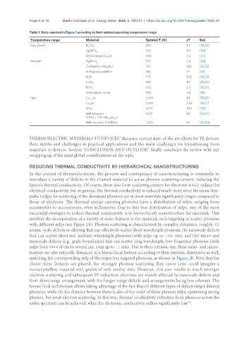
Table 1. Data reported in Figure 1 according to their optimal operating temperature range
Temperature range Material Optimal T (K) zT Ref.
Near Room Bi Te 3 320 1.4 [19,20]
2
AgSbTe 320 1.5 [14]
2
Iodine-doped Cu Se 400 2.3 [21]
2
Medium AgSbTe 573 2.6 [14]
2
Zintl phase (Mg Sb ) 725 1.65 [15,22]
2
3
SnSe polycrystalline 783 3.1 [12]
InSb 773 1.28 [15,23]
CoSb 3 835 1.9 [15,24]
PbTe 820 2.2 [15,25]
SnSe single crystal 923 2.6 [18]
High Cu Se 1,000 1.5 [15,26]
2-x
Cu Se 1,030 2.62 [15,27]
2
SiGe 1,073 1.84 [28]
Half-Heuslers 1,073 1.0 [15,29]
((Hf,Zr, Ti)CoSb Sn )
0.8 0.2
Half-Heuslers (FeNbSb) 1,200 1.5 [15,30]
THERMOELECTRIC MATERIALS TO DEVICES" discusses current state-of-the-art efforts for TE devices:
their merits and challenges in practical applications and the main challenges for transitioning from
materials to devices. Section "CONCLUSION AND OUTLOOK" finally concludes the review with our
wrapping up of the main global considerations on the topic.
REDUCING THERMAL CONDUCTIVITY BY HIERARCHICAL NANOSTRUCTURING
In the context of thermoelectricity, the process and consequence of nanostructuring is essentially to
introduce a variety of defects in the channel material to act as phonon scattering centers, reducing the
lattice's thermal conductivity. Of course, these also form scattering centers for electrons which reduce the
electrical conductivity, but in general, the thermal conductivity is reduced much more since the mean-free-
paths (mfps) for scattering of the dominant phonons are in most materials significantly longer compared to
those of electrons. The thermal energy-carrying phonons have a distribution of mfps, ranging from
nanometers to micrometers, even millimeters. Due to this vast distribution of mfps, one of the most
successful strategies to reduce thermal conductivity is to hierarchically nanostructure the materials. This
involves the incorporation of a variety of nano-features in the material, each targeting to scatter phonons
with different mfps (see Figure 2A). Phonon scattering is characterized by complex dynamics, roughly: (i)
atomic-scale defects or alloying that can effectively scatter short wavelength phonons, (ii) nanoscale defects
that can scatter short and medium wavelength phonons (with mfps up to ~100 nm), and (iii) micro and
mesoscale defects (e.g., grain boundaries) that can scatter long wavelength, low-frequency phonons (with
mfps from 100 s of nm to several μm, even up to ~1 mm). Due to their intrinsic size, these nano- and micro-
features are also naturally distanced in a hierarchical fashion according to their intrinsic dimension as well,
matching the corresponding mfp of the respective targeted phonons, as shown in Figure 2B. Note that the
closer these features are placed, the stronger phonon scattering they cause (one could imagine a
nanocrystalline material with grains of only several nm). However, this also results in much stronger
electron scattering and subsequent PF reduction; electrons are mainly affected by nanoscale defects and
their short-range arrangement, with the longer-range defects and arrangements being less relevant. The
hierarchical architecture allows taking advantage of the fact that (i) different types of defects target distinct
phonons, while (ii) the distance between them is also of the order of those phonon mfps, optimizing strong
phonon, but weak electron scattering. In this way, thermal conductivity reduction from phonons across the
[37]
entire spectrum can be achieved, while the electronic conductivity suffers significantly less .