
Page 150 - Read Online
P. 150
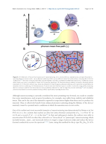
Martin-Gonzalez et al. Energy Mater. 2025, 5, 500121  https://dx.doi.org/10.20517/energymater.2025.32  Page 5 of 35


                Figure 2. (A) Schematic of hierarchical (panoscopic) nanostructuring, where atomic defects, nanoinclusions, and grain boundaries -
                spanning atomic to macro scales - act as phonon scattering centers across different mean-free-paths (mfps), reducing lattice thermal
                conductivity [35] . The lower color plot illustrates typical frequency and mfp contributions to thermal conductivity. Combining various
                defect types and sizes is essential to target the full phonon spectrum. (B) Nanostructured material schematic showing optimal
                placement of: (1) Atomistic defects (e.g., vacancies, dopants) for high-frequency phonon scattering, with controlled concentrations to
                minimize electron scattering; (2) Nanoinclusions of varied sizes and interface types to scatter a wide mfp range while preserving
                electron transport; and (3) Grain boundaries in nanocrystalline materials for mid- to long-mfp phonon  scattering [36] , with secondary
                phases at boundaries to enhance phonon blocking without significantly impeding electron flow.


               Although nanostructuring is currently considered the most promising way forward, one needs to consider
               that some nanofeatures, such as grain boundaries, for example, may suffer from stability and reliability
               issues. This can be the case if the material is exposed to temperatures higher than those used to produce the
               material. Thus, to effectively benefit from enhanced phonon scattering along the lifetime of the device/
               material, it must be operated under conditions at which the nanostructures do not evolve.

               One of the earliest and most successful examples of nanostructuring was demonstrated by Biswas et al. for
               PbTe in 2012, for a system that reached an ultra-low lattice thermal conductivity of κ  < 0.9 W·m ·K  at
                                                                                                    -1
                                                                                                       -1
                                                                                          p
               915 K and a record zT of ~ 2.2 at the time . In that and subsequent studies, the authors were able to
                                                     [17]
               nanostructure PbTe/SrTe in what they referred to as “hierarchical” or “panoscopic” nanostructuring, which
               included atomic-, nano-, and mesoscale defects to target a range of phonon mfps and reduce the lattice
               thermal conductivity across the spectrum [17,38,39] . Later, using this method for the p-type Pb Na Te-SrTe
                                                                                             0.98
                                                                                                 0.02