
Page 155 - Read Online
P. 155
Page 10 of 35 Martin-Gonzalez et al. Energy Mater. 2025, 5, 500121 https://dx.doi.org/10.20517/energymater.2025.32
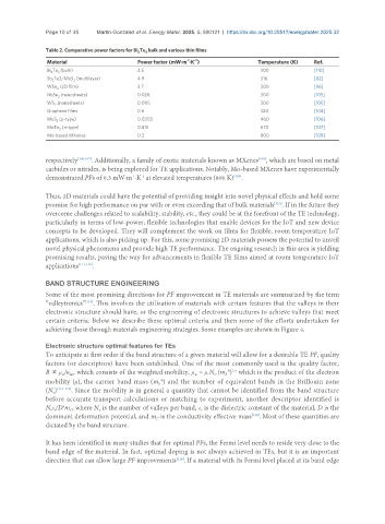
Table 2. Comparative power factors for Bi Te bulk and various thin films
2
3
Material Power factor (mW·m ·K ) Temperature (K) Ref.
-2
-1
Bi Te (bulk) 4.5 300 [110]
2
3
Sb Te3/MoS (multilayer) 4.9 316 [82]
2 2
WSe (2D film) 3.7 300 [96]
2
NbSe (nanosheets) 0.026 300 [105]
2
WS (nanosheets) 0.005 300 [105]
2
Graphene films 0.6 320 [104]
MoS (p-type) 0.0303 460 [106]
2
MoTe (n-type) 0.815 670 [107]
2
Mo-based MXenes 0.3 800 [109]
[108]
respectively [106,107] . Additionally, a family of exotic materials known as MXenes , which are based on metal
carbides or nitrides, is being explored for TE applications. Notably, Mo-based MXenes have experimentally
demonstrated PFs of 0.3 mW·m ·K at elevated temperatures (800 K) .
-1
-2
[109]
Thus, 2D materials could have the potential of providing insight into novel physical effects and hold some
promise for high performance on par with or even exceeding that of bulk materials . If in the future they
[110]
overcome challenges related to scalability, stability, etc., they could be at the forefront of the TE technology,
particularly in terms of low-power, flexible technologies that enable devices for the IoT and new device
concepts to be developed. They will complement the work on films for flexible, room temperature IoT
applications, which is also picking up. For this, some promising 2D materials possess the potential to unveil
novel physical phenomena and provide high TE performance. The ongoing research in this area is yielding
promising results, paving the way for advancements in flexible TE films aimed at room temperature IoT
applications [111,112] .
BAND STRUCTURE ENGINEERING
Some of the most promising directions for PF improvement in TE materials are summarized by the term
[113]
“valleytronics” . This involves the utilization of materials with certain features that the valleys in their
electronic structure should have, or the engineering of electronic structures to achieve valleys that meet
certain criteria. Below we describe these optimal criteria and then some of the efforts undertaken for
achieving those through materials engineering strategies. Some examples are shown in Figure 4.
Electronic structure optimal features for TEs
To anticipate at first order if the band structure of a given material will allow for a desirable TE PF, quality
factors (or descriptors) have been established. One of the most commonly used is the quality factor,
B μ /κ , which consists of the weighted mobility, μ = μ.N .(m *) which is the product of the electron
1.5
b
w
lat
w
v
mobility (μ), the carrier band mass (m *) and the number of equivalent bands in the Brillouin zone
b
(N ) [114-117] . Since the mobility is in general a quantity that cannot be identified from the band structure
v
before accurate transport calculations or matching to experiment, another descriptor identified is
2
N ε /D m , where N is the number of valleys per band, ε is the dielectric constant of the material, D is the
r
v r
v
C
dominant deformation potential, and m is the conductivity effective mass . Most of these quantities are
[118]
C
dictated by the band structure.
It has been identified in many studies that for optimal PFs, the Fermi level needs to reside very close to the
band edge of the material. In fact, optimal doping is not always achieved in TEs, but it is an important
[119]
direction that can allow large PF improvements . If a material with its Fermi level placed at its band edge