


Page 77 - Read Online
P. 77
Page 6 of 13                                                   Xia et al. Energy Mater. 2026, 6, 600022


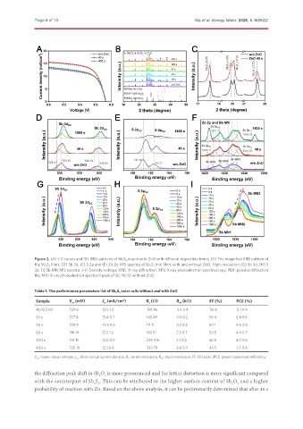
               Figure 2. (A) J-V curves and (B) XRD patterns of Sb 2 S 3  doped with ZnO with different deposition times; (C) The magnified XRD pattern of
               the Sb 2 S 3  films; (D) Sb 3d, (E) S 2p and (F) Zn 2p XPS spectra of Sb 2 S 3  thin films with and without ZnO. High-resolution (G) Sb 3d, (H) S
               2p, (I) Sb MN XPS spectra. J-V: Density-voltage; XRD: X-ray diffraction; XPS: X-ray photoelectron spectroscopy; PDF: powder diffraction
               file; MN: X-ray photoelectron spectrum peak of Sb; W/O: without ZnO.


               Table 1. The performance parameters list of Sb 2 S 3  solar cells without and with ZnO
               Sample       V oc  (mV)   J sc  (mA/cm )    R s  (Ω)   R sh  (kΩ)   FF (%)     PCE (%)
                                                 2
               W/O ZnO      729 6        12.5 1.2          158 86      3.2 0.4     56 6       5.1 0.9
               20 s         727 8        13.4 0.7          143 49     3.0 0.2      58 4       5.4 0.6
               40 s         728 9        14.6 0.6          111 11     3.2 0.2      59 1       6.6 0.3
               80 s         716 14       13.3 1.2          182 51     2.3 0.7      50 5       4.4 0.7
               200 s        715 15       12.0 0.9          238 106    2.1 0.5      46 5       4.0 0.5
               400 s        725 10       12.1 0.8          333 79     2.6 0.7      43 5       3.7 0.6
               V oc : Open-circuit voltage; J sc : short-circuit current density; R s : series resistance; R sh : shunt resistance; FF: fill factor; PCE: power conversion efficiency.

               the diffraction peak shift in Sb O  is more pronounced and the lattice distortion is more significant compared
                                        2
                                          3
               with the counterpart of Sb S . This can be attributed to the higher surface content of Sb O  and a higher
                                                                                              3
                                                                                            2
                                      2 3
               probability of reaction with Zn. Based on the above analysis, it can be preliminarily determined that after 40 s

