


Page 81 - Read Online
P. 81
Page 10 of 13                                                  Xia et al. Energy Mater. 2026, 6, 600022


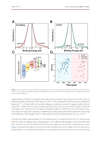
               Figure 4. UPS spectrum of (A) control and (B) Zn doping Sb 2 S 3  thin films; (C) schematic band diagram and (D) the summarized PCE of
               previous works of Sb 2 S 3  solar cell. UPS: Ultraviolet photoelectron spectroscopy; FTO: fluorine-doped tin oxide; CdS: cadmium sulfide; PCE:
               power conversion efficiency.


               single-function strategies. For instance, prior approaches to alleviate back-contact issues often relied on
               introducing distinct metal oxide buffer layers (e.g., WO , MoO ) primarily for hole transport or energy level
                                                             3-x
                                                                    2
               alignment [13,17] , or focused solely on elemental doping (e.g., solution-processed Zn doping) to tailor electrical
               properties . While effective, these strategies typically address only one aspect of the complex interfacial
                        [16]
               challenges in Sb S -based devices. Our approach uniquely integrates a diffusion barrier and a dopant source
                            2 3
               into a single sub-nanometer-scale layer, simultaneously tackling phase purity, defect passivation, and energy
               level modulation. This synergistic effect is evidenced by the concurrent improvement in N , R , and V .
                                                                                          A
                                                                                             rec
                                                                                                     oc
               Through the strategic implementation of a ZnO protective layer, we optimized both the Sb O  thickness and
                                                                                              3
                                                                                            2
               achieved surface Zn-doping in Sb S , culminating in a 7.00%-efficient, fully inorganic carbon-electrode-based
                                           2 3
               Sb S  solar cell with an FTO/CdS/Sb S /PbS/Carbon/Ag architecture. Statistically compiled literature data
                 2 3
                                              2 3
               [Figure 4D] position this efficiency at the state-of-the-art performance tier for planar Sb S  thin-film devices
                                                                                         2 3
               {Surpassing the 7% benchmark indicated by the gray dashed line, and the references are presented in

