


Page 78 - Read Online
P. 78
Xia et al. Energy Mater. 2026, 6, 600022                                          Page 7 of 13


               of ZnO deposition and subsequent annealing, Zn elements enter both the Sb S  and Sb O  lattices in the form
                                                                                          3
                                                                                       2
                                                                               2 3
               of substitutional doping, providing atomic-scale insights into the performance enhancement mechanism.
               X-ray photoelectron spectroscopy (XPS) was employed to elucidate the Zn chemical state. Survey scans
               [Supplementary Figure 5] confirmed elemental presence of C, Sb, S, O, and Zn. High-resolution Sb 3d
               spectra [Figure 2D] revealed that ZnO deposition reduced Sb O  content from 79% (control) to 65% (40 s
                                                                      3
                                                                    2
               ZnO), consistent with SEM/XRD trends. The S 2p spectrum [Figure 2E] showed typical spin-orbit splitting
               indicative of S  in Sb S , with a shift to higher binding energies upon ZnO deposition, suggesting reduced
                           2-
                                 2 3
               sulfur vacancies. Zn 2p peaks [Figure 2F] were absent in the control but faintly detected at 1,022.11 eV and
               1,045.50 eV in the 40 s ZnO sample. This chemically shift relative to crystalline ZnO indicates incorporation
               rather than phase separation. Concurrent shifts in Sb MNN Auger peaks further suggest Zn-S bonding and
               altered Sb electronic environments.

               To probe the depth distribution of Zn doping, XPS depth profiling was performed on the Zn-doping sample
               (40 s ZnO) versus the control (W/O ZnO) using Ar  sputtering at 0.03 nm/s. The Sb 3d  binding energy
                                                            +
                                                                                           5/2
               [Figure 2G] decreased with sputtering time, stabilizing beyond 200 s (~6 nm depth). Quantifying the Sb 3d 5/2
               shift relative to the unsputtered surface (Supplementary Figure 6, red spheres) showed an exponential decay
               (y = -0.91 + 0.73e ), with stabilization beyond 200 s (~6 nm depth). This confirms a thin Sb O  surface layer
                             -x/60
                                                                                             2
                                                                                               3
               serving as a hole-blocking but tunnel-permissive oxide. This structure is beneficial for suppressing interfacial
               recombination while enabling charge extraction. Concurrently, smaller S 2p shifts [Figure 2H and
               Supplementary Figure 6] and analogous Sb MNN Auger peak displacements (Figure 2I, Supplementary
               Figure 6, fit: y = -1.52 + 1.72e -x/42 ) indicate Zn  substitutional doping confined primarily to the top ~10 nm.
                                                     Sb
               Zn  substitution was confined to the top ~10 nm, supported by S 2p and Sb MNN trends [Figures 2H and I,
                 Sb
               Supplementary Figure 6]. This confirms that the ZnO cap limits Sb O  formation to an ultrathin ~6 nm layer,
                                                                         3
                                                                       2
               functioning as a wide-bandgap hole-blocking layer. Then it suppresses interfacial recombination while
               enabling efficient hole tunneling due to its minimal thickness, consistent with enhanced J . Collectively,
                                                                                             sc
               these depth-resolved analyses demonstrate the dual role of the ZnO interlayer: (1) restricting Sb O  to
                                                                                                     2
                                                                                                        3
               nanoscale surface regions, and (2) enabling shallow Zn doping in Sb S .
                                                                        2 3
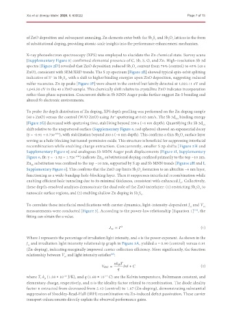
               To correlate these interfacial modifications with carrier dynamics, light-intensity-dependent J  and V oc
                                                                                                  sc
               measurements were conducted [Figure 3]. According to the power-law relationship [Equation 1] , the
                                                                                                     [19]
               fitting can obtain the α value.


                                                                                                        (1)
                                                                 ∝
               Where I represents the percentage of irradiation light intensity, and α is the power exponent. As shown in the
               J  and irradiation light intensity relationship graph in Figure 3A, yielded α = 0.90 (control) versus 0.91
               sc
               (Zn-doping), indicating marginally improved carrier collection efficiency. More significantly, the function
               relationship between V  and light intensity satisfies :
                                                          [20]
                                  oc

                                                             =         +                                (2)

               where T, k  (1.38 × 10  J/K), and q (1.60 × 10  C) are the Kelvin temperature, Boltzmann constant, and
                                  -23
                                                       -19
                        B
               elementary charge, respectively, and n is the ideality factor related to recombination. The diode ideality
               factor n extracted from decreased from 2.43 (control) to 1.87 (Zn-doping), demonstrating substantial
               suppression of Shockley-Read-Hall (SRH) recombination via Zn-induced defect passivation. These carrier
               transport enhancements directly explain the observed performance gains.

