


Page 79 - Read Online
P. 79
Page 8 of 13                                                   Xia et al. Energy Mater. 2026, 6, 600022


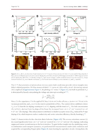
               Figure 3. (A) J sc , (B) V oc  as a function of light intensity (C) 1/C -V curves of Sb 2 S 3  devices; (D) Dark J-V curves and (E) Nyquist plots of
                                                         2
               Sb 2 S 3  devices; (F) Raman spectra of control and Zn doping Sb 2 S 3  thin films; (G and H) AFM images and (I and J) C-AFM images of control
               and Zn doping Sb 2 S 3  thin films. J-V: Density-voltage; V oc : open-circuit voltage; C-AFM: conductive atomic force microscopy; R tr : charge
               transport resistance; R rec : recombination resistance; J sc : short-circuit current density; R s : series resistance; C tr  and C rec : capacitor.


               The C-V characteristics of photovoltaic devices under dark conditions provide critical insights into
               defect-related properties. We thus measured dark C-V curves at 2 kHz with a 30 mV alternating current
               (AC) amplitude [Supplementary Figure 7]. By plotting 1/C  versus V [Figure 3C], the built-in potential (V )
                                                                 2
                                                                                                         bi
               is determined by linearly extrapolating the voltage axis intercept according to [21,22] :
                                                    1    2 (        −   )                               (3)
                                                       =
                                                     2     2
                                                                 0
               Here, C is the capacitance, V is the applied DC bias, S (0.09 cm ) is the cell area, ε 0 (8.854 × 10  F/cm) is the
                                                                    2
                                                                                              -14
               vacuum permittivity, and ε  (6.67) is the relative permittivity of Sb S . The control device exhibited a lower
                                      p
                                                                        2 3
               V  (1.13 V) than the Zn-doping counterpart (1.22 V), aligning with the trend in V . The hole concentration
                                                                                    oc
                bi
               (N ) of Sb S , derived from the slope of the linear fit, increased from 1.32 × 10  cm  (control) to 1.47
                                                                                     16
                                                                                          -3
                 A
                        2 3
               × 10  cm  (Zn-doping). This enhancement is attributed to shallow acceptor states (Zn ) induced by P-type
                      -3
                  16
                                                                                        Sb
               doping of Zn, which improves surface conductivity and carrier extraction efficiency, thereby boosting J sc [15] .
               Dark J-V characteristics further elucidate diode behavior [Figure 3D]. The reverse saturation current (J 0)
               decreased significantly from 5.06 × 10  mA/cm  (control) to 9.78 × 10  mA/cm  (Zn-doping), indicating
                                                        2
                                                                                    2
                                                -5
                                                                            -6
               suppressed carrier recombination at the back interface. To gain further insight into the underlying carrier
               recombination and transport dynamics, we performed EIS measurements under dark conditions and
               acquired the corresponding Nyquist plots (Figure 3E, inset showing the equivalent circuit). Among them, the

