
Page 23 - Read Online
P. 23
Page 4 of 20 Dang et al. Chem Synth 2023;3:14 https://dx.doi.org/10.20517/cs.2022.33
[51] [52]
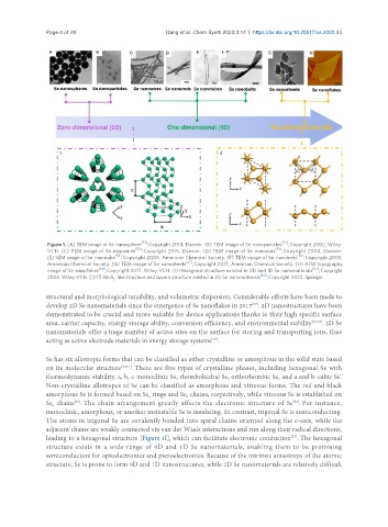
Figure 1. (A) TEM image of Se nanosphere ; Copyright 2014, Elsevier. (B) TEM image of Se nanoparticles ; Copyright 2002, Wiley-
[53] [54]
VCH. (C) TEM image of Se nanowires ; Copyright 2015, Elsevier. (D) TEM image of Se nanorods ; Copyright 2004, Elsevier.
[55] [56]
(E) SEM image of Se nanotube ; Copyright 2006, American Chemical Society. (F) TEM image of Se nanobelts ; Copyright 2005,
[57]
American Chemical Society. (G) TEM image of Se nanosheets ; Copyright 2017, American Chemical Society. (H) AFM topography
[58] [57]
image of Se nanoflakes ; Copyright 2017, Wiley-VCH. (I) Hexagonal structure existed in 0D and 1D Se nanomaterials ; Copyright
[60]
2002, Wiley-VCH. (J) 1T-MoS -like structure and square structure existed in 2D Se nanomaterials ; Copyright 2022, Springer.
2
structural and morphological tunability, and volumetric dispersion. Considerable efforts have been made to
develop 2D Se nanomaterials since the emergence of Se nanoflakes in 2017 . 2D nanostructures have been
[57]
demonstrated to be crucial and more suitable for device applications thanks to their high specific surface
area, carrier capacity, energy storage ability, conversion efficiency, and environmental stability [58,59] . 2D Se
nanomaterials offer a huge number of active sites on the surface for storing and transporting ions, thus
acting as active electrode materials in energy storage systems .
[59]
Se has six allotropic forms that can be classified as either crystalline or amorphous in the solid state based
on its molecular structure [60,61] . There are five types of crystalline phases, including hexagonal Se with
thermodynamic stability, a, b, c-monoclinic Se, rhombohedral Se, orthorhombic Se, and a and b-cubic Se.
Non-crystalline allotropes of Se can be classified as amorphous and vitreous forms. The red and black
amorphous Se is formed based on Se rings and Se chains, respectively, while vitreous Se is established on
8
8
Se chains . The chain arrangement greatly affects the electronic structure of Se . For instance,
[63]
[62]
8
monoclinic, amorphous, or another metastable Se is insulating. In contrast, trigonal Se is semiconducting.
The atoms in trigonal Se are covalently bonded into spiral chains oriented along the c-axis, while the
adjacent chains are weakly connected via van der Waals interactions and run along their radical directions,
[57]
leading to a hexagonal structure [Figure 1I], which can facilitate electronic conduction . The hexagonal
structure exists in a wide range of 0D and 1D Se nanomaterials, enabling them to be promising
semiconductors for optoelectronics and piezoelectronics. Because of the intrinsic anisotropy of the atomic
structure, Se is prone to form 0D and 1D nanostructures, while 2D Se nanomaterials are relatively difficult