
Page 26 - Read Online
P. 26
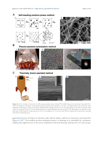
Dang et al. Chem Synth 2023;3:14  https://dx.doi.org/10.20517/cs.2022.33         Page 7 of 20


                Figure 3. (A) (i) Schematic illustration of self-seeding solution-phase  method [68] ; (ii) SEM image of Se nanowires; Copyright 2002,
                Wiley-VCH. (B) (i) Schematic of the plasma-assisted selenization  process [69] ; (ii) A top view SEM image of Se nanowires and a
                magnified TEM image of single Se nanowire with the lattice spacings of 0.351 nm of (110) and 0.502 nm of (001); Copyright 2018,
                American Chemical Society. (C) (i) Schematic illustration of thermally drawn-assisted method [70] ; (ii) SEM image of Se nanowire arrays
                and inset is TEM image of a single nanowire with 32 nm thickness; (iii) Cross-sectional SEM micrograph of Se nanowires; Copyright
                2011, Nature Publishing Group.


               approach has been developed to fabricate well-ordered, highly uniform Se nanowires and nanotubes
                           [70]
               [Figure 3C (i)] . This method involves multistep iterative co-drawing of Se embedded in a polymeric
               cladding that supports most of the stress resulting from thermal drawing. Starting with a Se macroscopic