Page 25 - Read Online
P. 25
Page 6 of 20                         Dang et al. Chem Synth 2023;3:14  https://dx.doi.org/10.20517/cs.2022.33


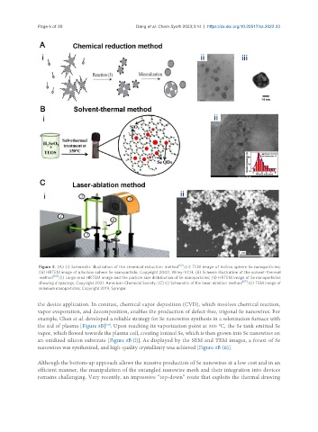
                Figure 2. (A) (i) Schematic illustration of the chemical reduction  method [52] ; (ii) TEM image of hollow sphere Se nanoparticles;
                (iii) HRTEM image of a hollow sphere Se nanoparticle; Copyright 2002, Wiley-VCH. (B) Scheme illustration of the solvent-thermal
                method [64] ; (i) Large-area HRTEM image and the particle size distribution of Se nanoparticles; (ii) HRTEM image of Se nanoparticles
                showing d spacings; Copyright 2021, American Chemical Society. (C) (i) Schematic of the laser-ablation method [65] ; (ii) TEM image of
                selenium nanoparticles; Copyright 2019, Springer.

               the device application. In contrast, chemical vapor deposition (CVD), which involves chemical reaction,
               vapor evaporation, and decomposition, enables the production of defect-free, trigonal Se nanowires. For
               example, Chen et al. developed a reliable strategy for Se nanowires synthesis in a selenization furnace with
               the aid of plasma [Figure 3B] . Upon reaching its vaporization point at 300 °C, the Se tank emitted Se
                                         [69]
               vapor, which flowed towards the plasma coil, creating ionized Se, which is then grown into Se nanowires on
               an oxidized silicon substrate [Figure 3B (i)]. As displayed by the SEM and TEM images, a forest of Se
               nanowires was synthesized, and high-quality crystallinity was achieved [Figure 3B (ii)].


               Although the bottom-up approach allows the massive production of Se nanowires at a low cost and in an
               efficient manner, the manipulation of the entangled nanowire mesh and their integration into devices
               remains challenging. Very recently, an impressive “top-down” route that exploits the thermal drawing

